
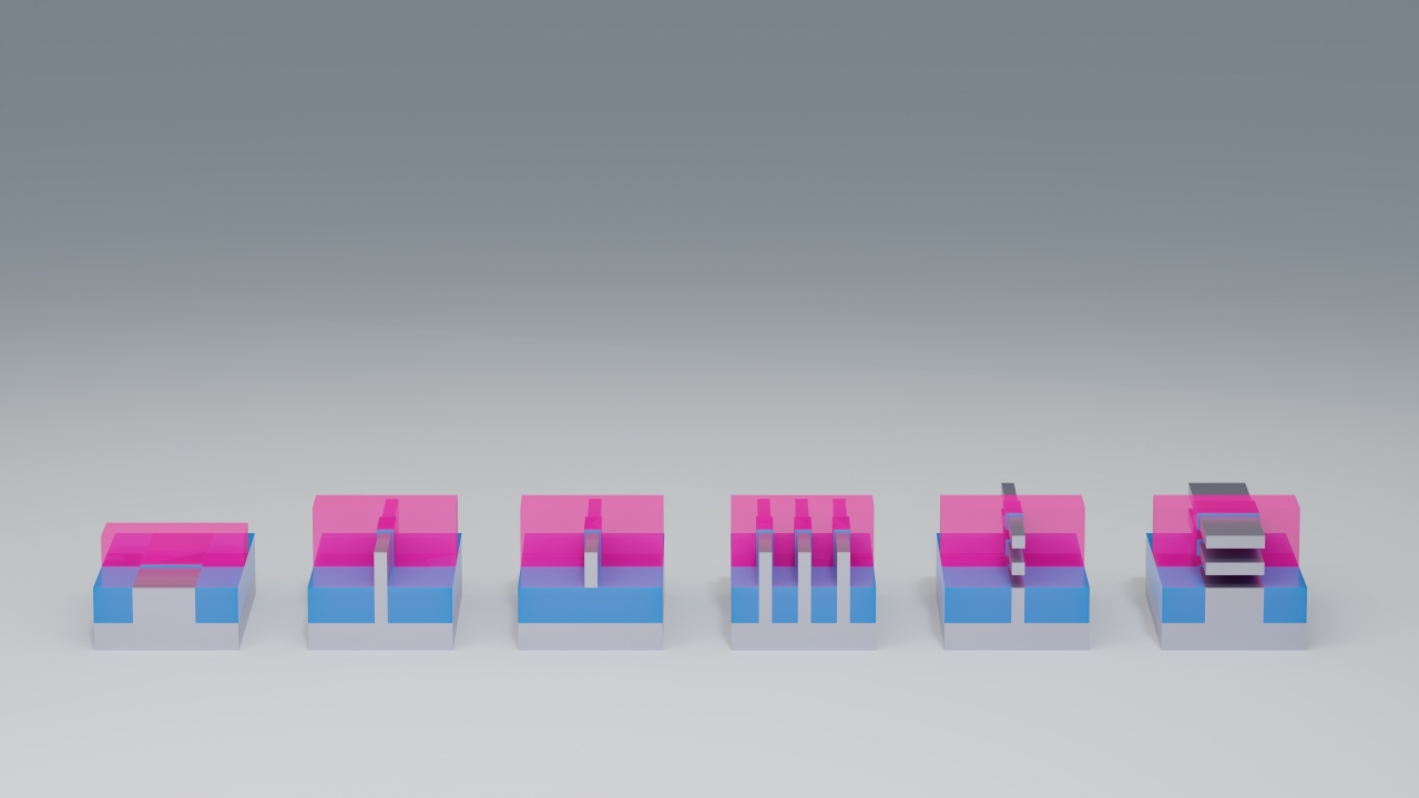
【1】What Is a Leading-Edge Node?
A leading-edge node refers to a technology node — a generational label describing a semiconductor’s level of miniaturization.
Examples: 7nm → 5nm → 3nm → 2nm → 1.4nm, and so on.
However, today’s “nm” figures no longer correspond directly to actual physical gate length, as they once did. They function more as a generational brand name than a literal measurement.
Even so, these numbers still carry real meaning, reflecting technological progress in areas such as:
・Shrinking line widths and gate pitch
・Increasing wiring density
・Reduced power consumption
・Improved performance (operating frequency)
【2】Why Miniaturization Continues to Become More Difficult
The industry was able to progress from 7nm down to 5nm using FinFET technology, but below 3nm, physical limits begin to come into view.
Key reasons include:
(1) Short-channel effects
As the channel becomes too short, controlling current flow becomes increasingly difficult.
(2) Increasing leakage current
As the insulating layer becomes thinner, electrons increasingly tunnel through it.
(3) Variability becomes a major problem
At scales where individual atoms matter, structural variation directly affects device characteristics.
(4) The resistance/capacitance (RC) wall
As wiring becomes thinner, both increasing resistance and increasing wiring delay (RC delay) become significant problems.
In short, the conventional rules that once governed miniaturization no longer hold.
【3】The Transition From FinFET to GAA (Gate-All-Around)
Below the 2nm node, FinFET technology reaches its own limits.
The reason: FinFET’s gate can only control the channel from three sides.
This is where GAA (Gate-All-Around) technology comes in.
Characteristics
・The gate completely surrounds the channel, covering all 360 degrees.
・Leakage current is dramatically reduced.
・Control remains strong even as devices shrink further.
・Significantly outperforms FinFET in both performance and power efficiency.
TSMC, Samsung, and Intel all plan to adopt GAA technology across the 2nm to 1.4nm generations.
【4】Comparing the Technical Characteristics of 3nm, 2nm, and 1.4nm 3nm (the final FinFET generation, with some GAA adoption)
3nm (the final FinFET generation, with some GAA adoption)
・The limits of miniaturization begin to come into view.
・Wiring resistance becomes an increasingly dominant factor.
・Power efficiency improves, but performance gains become more modest.
2nm (full-scale GAA adoption)
・Channel control improves dramatically.
・Power efficiency improves significantly, by roughly 20–30%.
・Transistor counts increase sharply.
・Becomes the mainstream node for AI chips.
1.4nm (the entry point to the post-GAA era)
・Further optimization of GAA becomes essential, as controlling extremely narrow nanosheets becomes increasingly difficult.
・Copper wiring approaches its own limits, with rising resistance.
・The physical limits of EUV lithography draw ever closer.
・Discussion begins around new materials and structures, such as CFET and 2D materials.
【5】Why the Industry Continues to Pursue Leading-Edge Nodes
(1) The explosive power demands of AI chips
Power density has increased more than tenfold compared with earlier generations. Continued miniaturization — and the resulting reduction in power consumption and improvement in performance — has become essential.
(2) The cost structure of servers and data centers
Power and cooling costs have become a major bottleneck.
(3) Battery life in smartphones and PCs
Achieving the same performance at lower power consumption has become essential.
(4) Competitiveness among semiconductor companies
This is the arena in which TSMC, Samsung, and Intel compete for industry leadership — and continued miniaturization is directly tied to national strategic interests as well.
【6】Major Challenges at Leading-Edge Nodes
・Achieving uniformity in GAA structures (controlling nanosheet width precisely)
・The difficulty of high-aspect-ratio etching
・Wiring resistance — copper is approaching its limits, prompting consideration of alternatives such as ruthenium
・Declining reliability of low-k materials
・Stochastic defects unique to EUV lithography
・Rapidly increasing power density (heat generation)
・The growing complexity introduced by chiplet architectures
At present, the “wiring wall” and the “thermal wall” stand out as the two most significant challenges facing the industry.
【7】Comparing TSMC, Samsung, and Intel's Leading-Edge Nodes
TSMC
・The world’s largest semiconductor foundry.
・Progressing from 3nm to 2nm (GAA) and on to 1.4nm.
・High yield remains its greatest strength.
Samsung
・Was first to introduce GAA at the 3nm node.
・However, has faced reported challenges around yield.
・A comprehensive manufacturer, with both memory and logic businesses.
Intel
・Pursuing a resurgence through its “IDM 2.0” strategy.
・Progressing from its 20A node (roughly equivalent to 2nm) to 18A (roughly equivalent to 1.8nm).
・Has announced plans to be among the first to adopt high-NA EUV lithography.
【8】Looking Ahead: What Happens Below 1nm?
Candidate technologies for this future include:
・CFET (Complementary FET): A structure that stacks the nFET and pFET vertically, one atop the other.
・2D materials (such as MoS₂): Using atomically thin channel layers to suppress short-channel effects.
・Convergence with optical computing.
・The entry into quantum-scale technologies.
Rather than marking the end of miniaturization altogether, this represents the beginning of an era in which the very methods of miniaturization are fundamentally changing.
【9】Summary
・A leading-edge node is a technical designation representing a generation of miniaturization.
・Below 3nm, FinFET reaches its limits, and GAA technology takes over to push further.
・At 1.4nm, both EUV lithography and available materials are approaching their own limits.
・Demand from AI and data centers continues to drive the push toward further miniaturization.
・Wiring resistance and heat generation stand as the two greatest barriers.
・The future points toward CFET, 2D materials, and increasingly three-dimensional structures.
Comprehension Check
1.Why does FinFET struggle below the 2nm node?
2.What is the greatest advantage of GAA technology?
3.Why does wiring resistance become such a significant problem at leading-edge nodes?
Column Supervisor: Koji Kakumoto (Otis Group Co., Ltd.)
After studying abroad and working in planning and development at a trading company, he joined Otis Group Co., Ltd. in 2011. While primarily working in the Corporate Planning Department, he has also served concurrently in manufacturing and technical divisions, and since 2018 has served as Representative Director, working to drive business growth and strengthen the organization.
This article is a general technical explanation intended for educational purposes and does not refer to any specific company, product, or technology.