【1】What Is GAA (Gate-All-Around)?
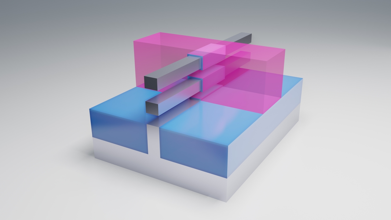
GAA is a transistor structure in which the gate completely surrounds the channel — the pathway current flows through — from all directions, covering the full 360 degrees.
While conventional FinFET technology could only control the channel from three sides, GAA’s fully surrounding gate gives it dramatically stronger current control.
This means that even as devices continue to shrink, GAA offers major advantages:
・Leakage current does not increase.
・Switching characteristics remain stable.
・Power efficiency remains high.
GAA is expected to become the mainstream structure from the 2nm node onward.
【2】Why the Industry Is Moving From FinFET to GAA
Reasons FinFET is reaching its limits:
(1) Insufficient channel control
As the fin (the raised structure) becomes thinner and shorter with continued miniaturization, the gate’s control weakens, making short-channel effects (SCE) increasingly severe.
(2) Growing variability
Fluctuations in the fin’s size and shape have an increasingly direct impact on device performance.
(3) Rising leakage current
The gate insulating layer can no longer be made any thinner.
GAA emerged as a structure specifically designed to solve these problems.
【3】What Is a Nanosheet Structure (NanoSheet / NanoRibbon)?
The nanosheet is the leading implementation of GAA technology.
A conceptual view of the structure
・Several thin, sheet-like (plate-shaped) channels are stacked on top of one another.
・The gate completely surrounds every one of these sheets.
・The width of each sheet corresponds to the effective channel width.
Characteristics
・Sheet width can be freely adjusted, making performance tuning easier.
・Multiple channels can be formed within the same footprint, improving performance.
・Offers greater current-driving capability than FinFET.
Samsung markets its implementation of this technology as MBCFET (Multi-Bridge Channel FET).
【4】Advantages of GAA
1. Unmatched electrical control
Because the gate surrounds the channel on all sides, short-channel effects are effectively suppressed.
2. A dramatic reduction in leakage current
Lower standby power consumption improves battery life.
3. Freedom to adjust channel width
Widening the sheet increases current; narrowing it reduces power consumption.
4. Improved area efficiency
Multiple channels can be stacked within the same footprint.
5. Meeting the high-current demands of AI and HPC applications
Essential for logic devices at the 2nm node and beyond.
If FinFET could be considered the reigning champion, GAA represents the champion of the future.
【5】The Manufacturing Difficulty of GAA (Its Biggest Barrier)
While the nanosheet GAA structure is excellent in principle, manufacturing it is extremely difficult.
Representative challenges
(1) Channel (sheet) uniformity
Even a difference of just a few nanometers in nanosheet width can significantly change a device’s current characteristics.
(2) Etching the stacked structure
Alternating layers of Si and SiGe must be selectively removed to form the individual sheets — a process requiring extremely advanced etching technology.
(3) Filling the gate
A uniform metal gate must be deposited into extremely narrow, nanoscale gaps between the stacked sheets.
(4) A sharp rise in wiring resistance
As wiring continues to shrink alongside the device itself, wiring — rather than the transistor — increasingly becomes the performance bottleneck.
(5) Thermal challenges
Higher current levels lead to increased heat generation, making accurate nanoscale thermal modeling increasingly important.
This is exactly why GAA is often described as “an ideal structure, but a manufacturing nightmare.”
【6】The State of GAA Development Worldwide (TSMC / Samsung / Intel)
Samsung
・Announced the world’s first mass production of GAA technology at the 3nm node.
・However, reports have pointed to ongoing yield challenges.
・Markets its technology under the MBCFET brand name.
TSMC
・Plans to adopt GAA at its 2nm (N2) node.
・Prioritizes stable, reliable yield above all else.
・Optimizing sheet count and width remains the key challenge.
Intel
・Introducing GAA technology (branded RibbonFET) at its 20A node.
・Has announced plans to be among the first to adopt high-NA EUV lithography as well.
・Views this technology as a key competitive advantage for its foundry business.
【7】What Comes After GAA (CFET and Beyond)
The leading candidate to succeed GAA is CFET (Complementary FET).
・Stacks the nMOS and pMOS vertically, one atop the other, rather than side by side.
・Dramatically improves area efficiency.
・Already under active research at companies such as Intel and IMEC.
Looking even further ahead, additional candidate technologies include:
・2D materials (such as MoS₂)
・Carbon nanotube FETs (CNT-FETs)
・Ferroelectric FETs
【8】Summary
・GAA is the next-generation structure designed to overcome the limits of FinFET.
・Its nanosheet structure dramatically improves electrical characteristics.
・It effectively suppresses leakage and short-channel effects caused by continued miniaturization.
・However, manufacturing it remains extremely difficult.
・Leading manufacturers are rolling out full-scale adoption across the 2nm to 1.4nm generations.
・CFET and 2D materials are the leading candidates for what comes next.
Comprehension Check
1.Briefly explain why GAA has become necessary in place of FinFET.
2.What is the greatest advantage of the nanosheet structure?
3.Name and explain the single most difficult step in manufacturing GAA devices.
Column Supervisor: Koji Kakumoto (Otis Group Co., Ltd.)
After studying abroad and working in planning and development at a trading company, he joined Otis Group Co., Ltd. in 2011. While primarily working in the Corporate Planning Department, he has also served concurrently in manufacturing and technical divisions, and since 2018 has served as Representative Director, working to drive business growth and strengthen the organization.
This article is a general technical explanation intended for educational purposes and does not refer to any specific company, product, or technology.