【1】The Role and Importance of Wafer Manufacturing
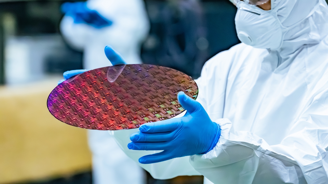
The wafer forms the foundation of a semiconductor device — it is the substrate onto which transistors and wiring are built. Factors such as:
・Flatness
・Crystal quality
・Impurity concentration
・Defect density
・Surface cleanliness
are said to determine as much as 90% of a product’s yield and performance, making wafer manufacturing an extraordinarily important step.
【2】Types of Wafer Materials
Three main materials are used for semiconductor wafers:
Silicon (Si)
・The most widely used material
・Inexpensive, with mature manufacturing technology
・Used broadly across CMOS, logic, and memory applications
Silicon carbide (SiC)
・Offers high voltage tolerance and heat resistance
・Used in EV inverters, industrial power supplies, and solar power conditioners
・The industry is transitioning to 8-inch wafers, a key factor in reducing costs
Gallium nitride (GaN)
・Well suited to high-speed, high-frequency applications
・Used in communications, fast charging, and data centers
・Typically formed as an epitaxial layer only, grown atop a silicon substrate
【3】The Silicon Wafer Manufacturing Process (the CZ Method)
The leading method for growing single-crystal silicon is the Czochralski (CZ) method.
The process proceeds as follows:
1.Polycrystalline silicon is melted in a crucible.
2.A seed crystal is brought into contact with the melt.
3.The crystal is slowly pulled upward as it grows.
4.A cylindrical ingot is formed.
5.The ingot is sliced into individual wafers.
6.The wafers are polished and cleaned to a mirror finish (CMP).
This is a mature process, and large-diameter (300mm) wafers are already in mass production.
【4】Epitaxial Growth
The epitaxial layer is a high-quality crystal layer used to reduce variation in transistor channel characteristics and resistance. Common types include:
・Silicon epitaxy
・SiGe epitaxy (used for high-speed, low-power applications)
・GaN epitaxy (typically grown on a silicon substrate)
Equipment used includes CVD furnaces (epi reactors) and MOCVD (for GaN).
【5】SiC Wafer Manufacturing (the Sublimation Method)
SiC is far harder than silicon, and its single-crystal manufacturing process is entirely different.
The leading method is the sublimation method, also known as Physical Vapor Transport (PVT):
1.SiC source material is sublimated at high temperature (around 2,000°C).
2.Vapor deposits onto a seed crystal, allowing the crystal to grow.
3.A thick SiC single crystal develops over time.
4.The crystal is then sliced, polished, and finished with CMP.
Because SiC is prone to defects, improving crystal quality and increasing wafer diameter (moving from 6-inch to 8-inch) remain the industry’s top priorities.
【6】GaN Wafer Manufacturing (Primarily Epitaxial Layer Formation)
Because growing large-diameter single crystals of GaN is difficult, unlike with SiC, GaN is generally used in one of the following structures:
・A GaN epitaxial layer grown via MOCVD atop a silicon substrate
・GaN grown atop a sapphire substrate
・GaN grown atop a SiC substrate (offering higher performance, but at higher cost)
Key priorities in GaN manufacturing include:
・Achieving low defect density
・Managing differences in thermal expansion between layers
・Improving characteristics for high-frequency applications
【7】Wafer Processing (Slicing → Polishing → Surface Treatment)
Once the single crystal has been grown, the following steps complete the wafer:
1.The ingot is sliced using a diamond blade.
2.Lapping (rough polishing) is performed.
3.Polishing brings the surface to a mirror finish.
4.CMP achieves nanometer-level flatness.
5.The wafer is cleaned with ultrapure water.
6.A cleanliness inspection checks for surface defects.
The flatness and cleanliness of the wafer surface directly affect the final performance of the resulting circuits.
【8】Key Points in Quality Control
Wafer quality directly affects the yield of subsequent manufacturing steps.
Key inspection items include:
・TTV (total thickness variation)
・Surface roughness (RMS)
・Crystal defect density (epi defect density)
・Particle contamination
・Metal contamination
・Bowing (uniformity of impurity concentration)
【9】Summary
・The wafer is the foundation of semiconductor manufacturing, and its quality directly determines yield.
・Si, SiC, and GaN are each used for clearly defined purposes.
・Si is used for general-purpose applications, SiC for high voltage tolerance, and GaN for high speed and high frequency.
・The quality of the epitaxial layer matters for both logic and power devices.
・The current major priorities are increasing wafer diameter for SiC and reducing defects for GaN.
Comprehension Check
1.What kind of process is the CZ method?
2.Why are SiC wafers so expensive?
3.Explain why GaN wafers are typically used in an “epitaxial layer” structure.
Column Supervisor: Koji Kakumoto (Otis Group Co., Ltd.)
After studying abroad and working in planning and development at a trading company, he joined Otis Group Co., Ltd. in 2011. While primarily working in the Corporate Planning Department, he has also served concurrently in manufacturing and technical divisions, and since 2018 has served as Representative Director, working to drive business growth and strengthen the organization.
This article is a general technical explanation intended for educational purposes and does not refer to any specific company, product, or technology.