【1】What Is Lithography?
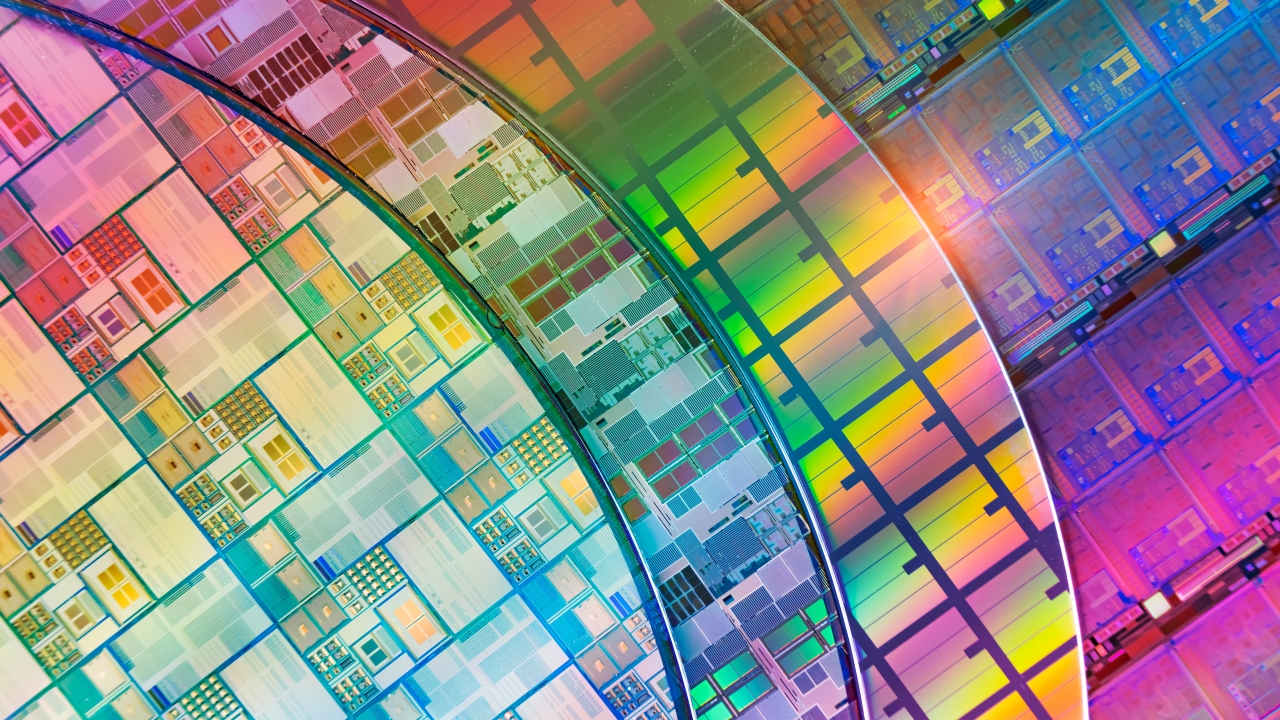
Lithography is the process of drawing extremely fine patterns — the circuitry itself — onto the surface of a wafer.
In semiconductor manufacturing, it is the core technology responsible for transferring a circuit design onto silicon — essentially, a projection process.
At the most advanced nodes, line widths are measured in just a few nanometers, and the performance of the lithography process directly determines the limits of miniaturization.
【2】Basic Steps of the Lithography Process
Lithography proceeds through the following steps:
1.Wafer cleaning (removing surface contamination)
2.Resist coating (via spin coating)
3.Soft baking (removing excess solvent)
4.Exposure (applying light)
5.Development (dissolving away the exposed — or unexposed — areas)
6.Hard baking (increasing the resist’s strength)
7.Subsequent processing (such as etching or ion implantation)
In short, the process can be summarized as: apply light to the resist, leave behind only the areas that are needed, and use that pattern as a mask.
【3】Types of Photoresist
The photoresist — the light-sensitive material — is the true star of lithography.
Positive resist
The areas exposed to light dissolve away. Well suited to fine line patterns.
Negative resist
The areas exposed to light harden and remain. Well suited to forming thicker films.
In the most advanced processes today, positive resist is the mainstream choice.
【4】Light Sources and Their Relationship to Miniaturization
Lithography’s performance is governed by the wavelength of light used — the shorter the wavelength, the finer the lines that can be drawn.
Representative light sources include:
・i-line (365nm)
・KrF (248nm)
・ArF (193nm)
・EUV (13.5nm) — the current state of the art
Today’s most advanced processes (3nm and 2nm) require EUV lithography.
【5】The Formula That Determines Resolution (the Rayleigh Equation)
The resolution limit of lithography is expressed by the following formula:
Minimum line width ≈ k₁ × (λ / NA)
・λ: the wavelength of light
・NA: the numerical aperture of the lens (larger is better)
・k₁: a process-dependent coefficient that can be reduced through process innovation (progressively lowered from 0.25 to 0.2 to 0.15)
The history of miniaturization has, in many ways, been a continuous effort to shorten λ, increase NA, and reduce k₁.
【6】Characteristics of EUV (Extreme Ultra Violet) Lithography
Key points about EUV (13.5nm), the technology at the center of modern lithography:
・Its extremely short wavelength enables very high resolution.
・Because EUV light is absorbed by air, a vacuum environment is required.
・It relies on a reflective mirror system, since conventional lenses cannot be used.
・The light source’s relatively weak output makes throughput a challenge.
・Ensuring the resist’s resistance to EUV exposure is also a significant challenge.
The price of a single EUV machine runs into the tens of billions of yen — an order of magnitude beyond conventional lithography tools.
【7】Multi-Patterning Technology
Before EUV became available, wavelength limitations meant that ArF light sources had to be pushed to their limits to draw fine lines. This gave rise to techniques such as:
・LELE (double exposure and double etching)
・SADP (Self-Aligned Double Patterning)
・SAQP (Self-Aligned Quadruple Patterning)
These are, in effect, process-based techniques for compensating for the limits of optics. Even with EUV now available, these techniques have not disappeared entirely.
【8】Alignment Technology
A chip’s circuitry is built up from dozens of stacked layers. Because of this, the technology that ensures each new layer aligns precisely with the layer beneath it — known as alignment — is critically important.
Misalignment can directly lead to:
・Wiring short circuits
・Variation in transistor characteristics
・Reduced yield
【9】Challenges That Grow With Further Miniaturization
As lithography continues to shrink, new challenges continue to emerge:
・Thinner resist layers becoming prone to pattern collapse
・Line width roughness (LWR) caused by light scattering
・Difficulty achieving proper light incidence on 3D structures
・Performance degradation caused by rough or uneven pattern edges
・Throughput challenges with EUV
・Difficulty detecting mask defects
In truth, the limits of miniaturization stem not only from optics, but also from the limits of resist materials and process technology.
【10】The Latest Trend: High-NA EUV
The next generation of lithography is High-NA EUV.
・Expands the numerical aperture from the conventional 0.33 to 0.55.
・Aims to support mass production at nodes below 2nm.
・Requires an overhaul of masks, resists, and processes alike.
Full-scale mass production is expected to begin around 2026–2027.
【11】Summary
・Lithography is the process of drawing circuitry, making it the heart of semiconductor manufacturing.
・Shorter wavelengths of light enable higher resolution.
・EUV, at 13.5nm, represents the current state of the art, though it still faces significant challenges around light intensity and mask defects.
・High-NA EUV is the key to the next generation of lithography.
・Miniaturization is a combined battle fought across optics, materials, and process technology.
Comprehension Check
1.Explain the purpose of lithography in a single sentence.
2.What happens as wavelength shortens — for example, from 193nm to 13.5nm?
3.Name one major challenge facing EUV equipment.
Column Supervisor: Koji Kakumoto (Otis Group Co., Ltd.)
After studying abroad and working in planning and development at a trading company, he joined Otis Group Co., Ltd. in 2011. While primarily working in the Corporate Planning Department, he has also served concurrently in manufacturing and technical divisions, and since 2018 has served as Representative Director, working to drive business growth and strengthen the organization.
This article is a general technical explanation intended for educational purposes and does not refer to any specific company, product, or technology.