【1】Beyond 2nm, Scaling Becomes a Battle Against Physical Limits
Semiconductor scaling has moved from “an era in which shrinking dimensions raises performance” → “an era of advancing by outwitting physics.”
The problems that become pronounced from 2nm onward are:
・A sharp increase in quantum tunneling current
・Weakening gate control (the limits of electrostatics)
・A sharp rise in wiring resistance (higher R → worse RC delay)
・Declining material reliability (embrittlement of ULK, EM degradation of Cu)
・The EUV resolution limit (the 13.5nm wavelength barrier)
In other words, the limits of scaling stand in the way as real-world constraints.
【2】The Physical Limits of EUV and the Future of High-NA
EUV is the most important technology supporting semiconductors, but its limits are coming into view.
Main bottlenecks:
・Mask blur
・Losses in the multilayer films of the reflective mirrors
・Stochastic noise during exposure (stochastic defects)
・Dimensional fluctuations caused by shot noise
High-NA (NA = 0.55) pushes resolution higher, but it is said to be effectively the last remaining headroom.
Candidates to go beyond EUV are:
・Shorter-wavelength EUV (6.x nm)
・EUV combined with electron beams (hybrid)
・Next-generation mask technology (phase-shift EUV)
However, all of them are still far from practical use.
【3】"Three New Paradigms" Replacing Scaling
(1) Backside Power Delivery
Now that wiring delay is approaching its limits, a fundamental structural reform is underway: moving the power wiring to the back side.
Advantages:
・Significant reduction in power IR drop
・Less power supply noise
・Greater freedom in front-side wiring
Intel (PowerVia), TSMC, and Samsung are competing for leadership.
(2) 3D Transistors (CFET / 3D Sequential)
After GAA comes CFET (Complementary FET).
・NMOS and PMOS are stacked vertically
・Zero distance between transistors
・Area reduction and performance improvement advance at the same time
Beyond that:
・Monolithic 3D
・3D sequential integration
・Wafer-to-wafer bonding
From the limits of the plane → to an era of escaping in the vertical direction.
(3) Chiplets × Advanced Packaging
The most promising way to improve performance without relying on scaling.
・CoWoS
・SoIC
・Foveros
・EMIB
・HBM4/5
Instead of the conventional “giant SoC,” structures that are divided and then stacked and combined (the Lego model) will become mainstream.
【4】The Limits of Materials and the Rise of "Post-Si Materials"
Because we have entered a region where physics no longer allows dimensions to shrink further, efforts to upgrade the materials themselves are accelerating.
Main candidates:
・2D materials (MoS₂, WS₂, graphene)
・CNTs (carbon nanotube FETs)
・Ferroelectric transistors (FeFETs)
・Next-generation Low-k (air gaps, nanoporous materials)
・Replacing Cu with Ru/Co/Mo
However, the biggest barriers are:
・Stability in volume production
・Reliability (especially for ULK materials)
・Compatibility with existing equipment
・Cost
Materials engineering has once again become the main driver of semiconductor evolution.
【5】The Thermal Wall
The power density of AI chips and GPUs is rising sharply, and we have entered an era in which performance is limited by heat.
Technologies that will be needed:
・High-thermal-conductivity materials (graphite, diamond)
・Direct liquid cooling
・Backside cooling
・Heat removal through TSVs
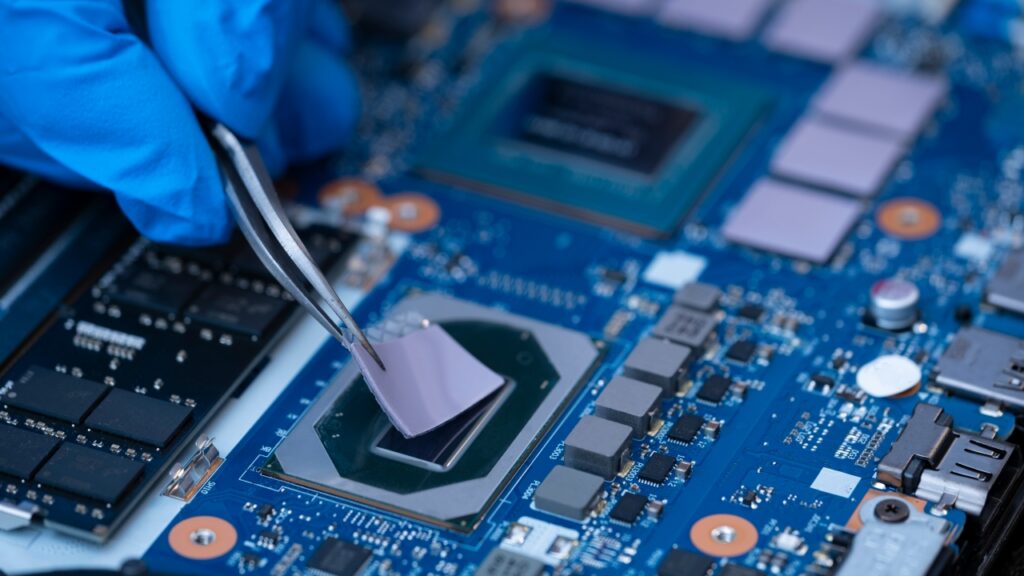
・Evolution of TIMs (higher-performance interface materials)
Unless the heat problem is solved, performance will not improve no matter how many transistors are added.
【6】The Emergence of Quantum Effects
Near the atomic scale, transistors enter “the world of statistics.”
Examples:
・Tunneling current
・Variability (a sharp increase in randomness)
・RTN (Random Telegraph Noise)
・Fluctuations in device lifetime
For this reason, designs that combine physical simulation × AI × statistical models are becoming essential.
【7】Quantum, Photonic, and Brain-Inspired Devices Advancing in Parallel
(1) Quantum Devices
Error correction is the key. Applications are still limited.
(2) Silicon Photonics
The leading candidate for optical interconnects that go beyond the limits of copper wiring. Expanding rapidly in AI data centers.
(3) Neuromorphic Computing
A brain-inspired architecture. Because computation and memory take place in the same location, lower power consumption is possible.
【8】Summary: Entering an Era of Breaking Through Limits
・Scaling is colliding head-on with physical limits
・EUV will also reach its limits within a few generations
・The challenges are “wiring resistance, current density, and heat”
・The solutions are “3D integration, chiplets, and materials evolution”
・New paradigms (quantum, photonic, brain-inspired) are progressing at the same time
・Semiconductors are shifting from technologies that shrink → to technologies that stack, divide, and change the physics
Comprehension Check
1.What is the most pronounced physical constraint from 2nm onward?
2.What does High-NA EUV solve, and what are its limits?
3.Explain the advantages of the CFET structure.
Column Supervisor: Koji Kakumoto (President, OTIS Co., Ltd.)
After studying abroad and working in planning and development at a trading company, he joined OTIS Co., Ltd. in 2011. While primarily working in the Corporate Planning Department, he has also served concurrently in manufacturing and technical divisions, and since 2018 has served as President, working to drive business growth and strengthen the organization.
This article is a general technical explanation intended for educational purposes and does not refer to any specific company, product, or technology.