
■ Why Have Semiconductors Started to Stack Up?
Until now, semiconductors have evolved mainly in the planar direction.
In other words, they have improved performance through
● Miniaturization
● Higher density
● Circuit shrinking
In recent years, however, the limits of miniaturization alone have begun to appear.
That is why what is now advancing rapidly is going 3D.
■ What Are 3D Semiconductors?
Simply put, 3D semiconductors are a technology for stacking semiconductors.
For example, in
Memory
AI chips
GPUs
HBM
technologies for stacking multiple chips vertically are advancing.
This makes it possible to achieve
● Higher speed
● Smaller size
● Larger capacity
● Lower latency
In other words, going 3D is starting to become a technology indispensable in the AI era.
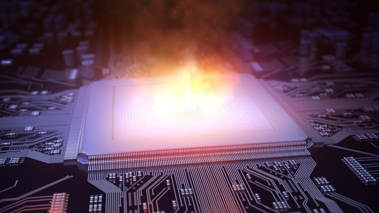
■ But When You Stack Them, Heat Cannot Escape
A major problem arises here.
Semiconductors generate heat when they operate.
In a planar structure, heat could be released sideways to some extent.
But when you go 3D, heat sources are stacked vertically.
In other words, you end up stacking hot things on top of each other.
This is extremely tough.
■ The Lower the Chip, the Worse It Gets
What is especially problematic is the bottom of the stack.
Because multiple chips sit on top, problems arise such as
● Heat becomes trapped
● Heat dissipation paths decrease
● Temperatures rise
● It becomes harder to cool
In other words, in future 3D semiconductors, what will matter more than how high the performance is
is how much heat can be released.
■ In the AI Era, Heat Density Rises Abnormally
In AI applications in particular, computing density is increasing sharply.
In other words, an enormous amount of power is concentrated in a small area.
As a result, heat density rises abnormally.
This is on a different level from conventional semiconductors.
■ Heat Stops Performance Itself
When semiconductors get hot,
● Reduced performance
● Increased noise
● Degradation
● Errors
● Shorter lifetime
can occur.
In other words, heat problems are not something you can dismiss as “a little hot.”
In the AI era, heat may stop performance itself.
■ That Is Why a Race for Thermal Solutions Is Under Way Around the World
Today, the semiconductor industry is researching various thermal solutions, such as
● TSV
● High thermal conductivity materials
● Vapor chambers
● Next-generation TIM
● Heat dissipation structures
● Liquid cooling
● High-precision assembly
In other words, future semiconductor competition is beginning to become not only a circuit competition
but also a heat competition.
■ The Researcher's Perspective
Structures that let heat escape become important
What will matter going forward includes
● Heat spreading
● Heat conduction
● Reducing contact resistance
● Stacked structures
● Material selection
● Optimizing heat dissipation paths
In other words, in future semiconductors, not only how to stack
but also how to release heat will be extremely important.
■ The Shop-Floor Perspective
Contact is harder than theory
On the actual shop floor, however, even more difficult problems arise.
For example,
● Tiny lifting
● Poor contact
● Steps at the level of a few μm
● Air layers
● Material deformation
● Differences in thermal expansion
● Assembly misalignment
In other words, “heat escapes in theory” and
“heat actually escapes in volume production” are completely different.
■ The Final 1mm of Heat Becomes Extremely Difficult
In 3D semiconductors,
● Thin
● Small
● High density
● Multilayer
all advance at the same time.
As a result, fine contact conditions become extremely important.
For example, even just
● Lifting of a few tens of μm
● A slight air layer
● Uneven contact
may greatly change thermal performance.
In other words, in future semiconductors, the difficulty of the final 1mm of heat will increase explosively.
■ What Matters from OTIS's Perspective
From OTIS’s perspective, what matters in the era of 3D semiconductors includes
● Microfabrication
● Thin-film processing
● High-precision lamination
● Contact between dissimilar materials
● High-precision die-cutting
● Lamination
● Contact stability
● Volume production stability
In particular, making high-performance materials work with high precision is important.
■ What OTIS Can Do
At OTIS, through
● Microfabrication
● High-precision die-cutting
● Thin-film processing
● High-precision lamination
● Processing of thermal management materials
● Stacking of irregular shapes
● Support for automated supply
we may be able to contribute to making thermal management functions work in volume production.
■ Outside OTIS's Expertise
On the other hand, OTIS is not a company that specializes in
● Semiconductor design
● AI chip development
● GPU design
● Semiconductor manufacturing equipment development
● Circuit design
However, in the area of making heat solutions work in volume production processes,
we may be able to play an important role.
■ Summary
The future of semiconductors will be a battle against heat
In the AI era, semiconductors will become even more
● High-performance
● Compact
● High-density
● Stacked
As a result, however, escape routes for heat are beginning to disappear.
In other words, future semiconductor competition may be decided not only by how much you can compute,
but by how well heat can be made to work.
And behind the scenes, technologies that support the final 1mm of heat will become increasingly important.
Column Supervisor: Koji Kakumoto (President, OTIS Co., Ltd.)
After studying abroad and working in planning and development at a trading company, he joined OTIS Co., Ltd. in 2011. While primarily working in the Corporate Planning Department, he has also served concurrently in manufacturing and technical divisions, and since 2018 has served as President, working to drive business growth and strengthen the organization.
This article is a general technical explanation intended for educational purposes and does not refer to any specific company, product, or technology.


