
■ Why Stack Semiconductors?
For a long time, improvements in semiconductor performance were achieved by making transistors smaller.
However, continuing to increase performance through miniaturization alone is becoming difficult both technically and economically.
So rather than making
● CPUs
● GPUs
● Memory
● I/O
● Communication circuits
all on one huge chip, the direction of
combining multiple chips and operating them as one system
is becoming important.
Chiplets.
2.5D integration.
3D integration.
HBM.
These are typical examples.
■ What Is 2.5D Integration?
In 2.5D integration, multiple chips are placed close together on top of
an interposer or the like.
For example,
GPU + HBM + HBM + HBM
are placed at high density on the same substrate.
The chips are not fully stacked vertically, but they can be connected at much shorter distances than in conventional board mounting.
Shorter wiring distances are advantageous for high-speed communication.
On the other hand, multiple high-heat components concentrate in a small area.
That is why the heat density of the entire package becomes high.
■ What Is 3D Integration?
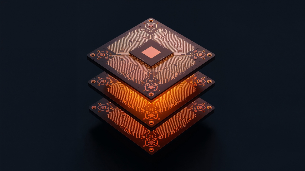
In 3D integration, chips are stacked vertically.
As an image, it is a structure of
Chip
↓
Chip
↓
Chip
↓
Substrate
The upper and lower chips are electrically connected by TSVs and the like.
This makes it possible to greatly shorten wiring distances.
From a thermal point of view, however,
chips stacked on top may block the exit for heat from the chips below.
This is the difficulty unique to 3D integration.
■ HBM Already Symbolizes the "Era of Stacking"
In AI semiconductors,
the importance of HBM is increasing rapidly.
HBM is memory that stacks multiple DRAMs vertically to enable high-speed, high-capacity data transfer.
By placing the GPU and HBM close together, the data needed for large volumes of AI computation can be supplied at high speed.
However,
the GPU generates heat.
The HBM also generates heat.
And they are placed very close to each other.
In other words, in AI semiconductors,
the increase in density for raising computing performance itself is making heat problems harder.
■ Conventional Thermal Management Was Basically "Release It Upward"
In a simple semiconductor package, heat can be released in
the Z direction
as in
Chip
↓
TIM
↓
Heat spreader
↓
TIM
↓
Heat sink
It was enough to place a cooling component on top of the heat-generating body.
In 3D integration, however, they are stacked as
Upper chip
↓
Middle chip
↓
Lower chip
From the point of view of an inner chip,
there is material above.
There is material below.
The distance and the number of interfaces before heat gets out increase.
■ The Further Inside a Chip Is, the Harder It Is to Cool
For example, suppose three chips are stacked.
The top chip is relatively close to the cooling component.
The middle chip, however, must release heat through
the upper chip,
the bonding layer,
the TIM,
and so on.
For the bottom chip, it becomes even more complex.
In other words,
even with the same heat generation, cooling conditions differ depending on stacking position.
In 3D integration, looking only at the “package temperature” becomes insufficient.
Hidden hot spots may form inside.
■ Being Reassured Just Because "the Average Temperature Is Low" Is Not Enough
Even if the average temperature of the entire package is low, only part of the inside may be hot.
For example,
an overall average of 70°C
may still mean
only part of the inside at 100°C.
This local high temperature may lead to
● Performance degradation
● Material degradation
● Degradation of joints
● Shorter service life
In other words, in 3D integration, what matters is not only what the temperature is,
but where it is what temperature.
■ Heat Does Not Pass Only Along the Shortest Path
Heat flows along paths with low thermal resistance.
That is why heat moves in multiple directions:
upward,
downward,
sideways.
Conventionally, the focus was on extracting heat in the Z direction.
As density increases, however, spreading heat in the XY direction also becomes important.
Here,
● Graphite
● Copper
● Vapor chambers
● Heat-spreading layers
become important.
■ Combining "Releasing Upward" and "Spreading Sideways"
In thermal management for 3D integration, rather than handling heat in one direction only, it is necessary to combine
releasing heat in the Z direction and spreading heat in the XY direction.
For example, there is the idea of
Heat-generating chip
↓
Thin TIM
↓
Heat-spreading layer
and from the heat-spreading layer,
→ Spreading heat sideways
→ Guiding heat to the enclosure or cooling components
In other words, a design is needed that not only gets heat out upward by the shortest distance, but releases it to places where there is room.
■ In 3D Integration, TIM Becomes Even More Important
TIM is a material that fills the fine gaps that exist between two solids.
In 3D integration, the number of interfaces increases.
For example, with
Chip
↓
TIM
↓
Heat spreader
↓
TIM
↓
Cooling component
there are multiple TIMs.
Each TIM has a slight thermal resistance.
Even if each one is small,
thermal resistances accumulate.
That is why
● TIM material
● TIM thickness
● Contact area
● Pressure
● Flatness
are important.
■ Thinner TIM Is Advantageous, but Too Thin Is Also Difficult
In general, for the same material, a thinner TIM makes it easier to reduce thermal resistance.
However, making it thinner may mean that
● It cannot absorb component warping
● It cannot fill surface roughness
● It cannot conform to steps
● The effect of dispensing/application variation becomes larger
In other words, there is the contradiction that thermally, you want it thinner.
For mounting, you want thickness.
In 3D integration, judgments on the order of tens of μm become important.
■ 0.1 mm Has Great Significance
For general mechanical parts, 0.1 mm looks like a very small difference.
In thin-film thermal design, however, it is different.
If, in a place where the TIM should be 0.1 mm,
lifting,
warping,
foreign matter,
or misalignment
creates an additional 0.1 mm gap,
the state of the heat path may change greatly.
This is exactly
“why a 0.1 mm lift ruins thermal performance,”
which we covered in 6-3.
The further 3D integration advances,
the more processing accuracy on the order of μm to 0.1 mm governs the performance of cooling components tens of mm in size.
■ Chip Warping Cannot Be Ignored Either
Semiconductor packages are not perfectly flat.
Different materials have different coefficients of thermal expansion.
Silicon.
Copper.
Resin.
Substrate.
TIM.
When the temperature changes, these expand and contract at different rates.
As a result,
the package warps.
When warping occurs,
the TIM is thin at the center.
The TIM is thick at the edges.
Or the reverse.
Then thermal resistance also varies by location.
■ Thermal Expansion Differences Also Affect Joints
In 3D integration, there are many fine joints.
The temperature rises.
It cools.
It rises again.
When this thermal cycle is repeated, stress arises from the difference in expansion of dissimilar materials.
In other words, the heat problem is not only
a problem of lowering temperature.
It is also
a problem of suppressing mechanical stress due to temperature changes.
Here too,
● Material selection
● Thickness
● Flexibility
● Adhesion
are important.
■ Achieving Insulation and Thermal Conduction at the Same Time
In semiconductors, parts that carry electricity and parts that must never carry it are close together.
That is why the requirement arises that
heat should pass through.
Electricity should not pass through.
So materials such as
● Ceramic-based thermally conductive materials
● Insulating TIM
● Insulating films
● Thermally conductive adhesives
are used.
However, adding insulating layers may make those layers thermal resistance.
Thinner is advantageous for heat.
But there is no longer any margin in insulation reliability.
Here too, there is a trade-off between thermal performance and insulation performance.
■ The "Edges" of Insulating Materials Become Important
It is not enough for an insulating material to be normal only in the center.
If the edges have
● Burrs
● Cracks
● Peeling
● Misalignment
it may affect electrical safety.
Especially as films become thinner, the condition of processed edges takes on relatively greater significance.
In other words, it is necessary to look not only at the insulation performance of the material,
but at the insulation performance after processing.
■ Graphite as a Heat-Spreading Material
Graphite has high thermal conductivity in the in-plane direction.
That is why it is well suited to applications that
spread local heat sideways.
For example,
Chip
↓
TIM
↓
Graphite
heat is spread into graphite larger than the chip.
From there, heat is handed to
● Metal frames
● Enclosures
● Heat sinks
● Cooling plates
In 3D integration,
the idea of using not only the area directly above the heat source but also the surrounding space as a heat path becomes important.
■ However, Graphite Also Has Weaknesses
Graphite is an excellent heat-spreading material, but it has characteristics such as
● Performance differs between the in-plane and thickness directions
● Thin materials are difficult to handle
● Powder may come off the edges
● It conducts electricity
● It can be mechanically easy to damage
That is why, in practice, it is sometimes combined with
● Insulating films
● Protective films
● Adhesives
Then, in turn, the laminated structure becomes important.
■ The Idea of Releasing Heat Sideways with Metal Foil
Copper foil and aluminum foil can also be used as materials for spreading heat.
Copper in particular has high thermal conductivity.
For example, a structure such as
Heat-generating body
↓
TIM
↓
Copper foil
→→→ Carrying heat to the enclosure side
can be considered.
Metal foils have the characteristics of being
● Thin
● Bendable
● Shape-processable
● Electrically conductive
That is why heat spreading and electrical functions can sometimes be combined.
On the other hand, because they are conductive, insulation design is needed.
■ What Is at the Destination Where Heat Is Released?
Even if heat is spread sideways with graphite or copper foil,
it is meaningless if there is no place to receive the heat beyond it.
For example, with
Chip
↓
TIM
↓
Graphite
→→→ Enclosure
the contact state between the graphite and the enclosure is also important.
If it is lifting here,
even though heat was carried sideways, it stops at the end.
In other words, in 3D integration, it is necessary
to create a continuous heat path from the heat source to the final heat discharge destination.
■ Combination with Vapor Chambers
When heat generation density becomes even higher, vapor chambers can be combined in addition to graphite and metal plates.
For example, a structure of
3D package
↓
TIM
↓
Vapor chamber
↓
Heat sink
The vapor chamber spreads local heat and then hands it to the heat sink.
Or it is combined with liquid cooling.
What matters is not which cooling technology is used,
but where heat is received, where it is carried, and where it is discarded.
■ Combination with Liquid Cooling
In high-heat AI semiconductors, the combination of 3D integration and liquid cooling is likely to become important.
For example, a structure of
3D package
↓
TIM
↓
Cold plate
↓
Coolant
Liquid cooling can carry a large amount of heat.
However, being liquid cooling does not mean interface problems disappear.
If the TIM is lifting,
heat does not reach the cold plate.
In other words, the more advanced the cooling technology, the more both
the performance of the cooling equipment and the quality of the interface are needed.
■ Summary
As we have seen, 3D integration is difficult because of the contradiction that chips one wants to bring closer electrically, one wants to keep apart thermally.
The more chips are stacked, the more heat sources crowd together, interfaces increase, and internal heat has difficulty getting out.
Releasing heat in the Z direction as before is not enough.
Graphite and metal foils that spread heat in the XY direction.
Vapor chambers that receive local heat over a surface.
Liquid cooling that can carry large amounts of heat.
Only by combining these is a path from the heat source to the heat discharge destination finally established.
However, whichever method is chosen, if the state of the interface, such as TIM thickness, contact pressure and warping, is poor, heat stops before it.
In other words, thermal management for 3D integration is not completed just by choosing excellent cooling technologies.
In Part 2, we look at how such thermal design is actually realized in volume production. We look at the processing challenges brought by thinner films, the difficulties of automation and inspection, and what role OTIS plays in this area.
Column Supervisor: Koji Kakumoto (President, OTIS Co., Ltd.)
After studying abroad and working in planning and development at a trading company, he joined OTIS Co., Ltd. in 2011. While primarily working in the Corporate Planning Department, he has also served concurrently in manufacturing and technical divisions, and since 2018 has served as President, working to drive business growth and strengthen the organization.
This article is a general technical explanation intended for educational purposes and does not refer to any specific company, product, or technology.



