【1】Introduction
Power devices are semiconductor devices designed to handle large currents and high voltages, efficiently controlling the flow of electrical power.
While CPUs and memory are dedicated to “processing information,” power devices are dedicated to “controlling the flow of electricity and handling power and energy” — making them essential to industrial equipment, home appliances, electric vehicles (EVs), and renewable energy systems.
【2】Characteristics of Power Devices
Unlike standard MOSFETs and BJTs, power devices need the following characteristics:
・High voltage tolerance (hundreds to thousands of volts)
・Support for large currents
・Low on-resistance (a reduced Rds(on))
・High-speed switching
・High-temperature operation (typically in the 150°C to 200°C range)
・High reliability and long service life
Because of these requirements, the materials and structures used differ significantly from those found in typical logic devices.
【3】Major Types of Power Devices
3-1. Power MOSFET
Characteristics
・Suited to low-to-medium voltages (30–900V)
・High-speed switching
・Low losses, high efficiency
・Used in DC-DC converters and motor control
Structure
・Trench MOS (a vertical gate structure) is the mainstream approach.
・Current flows vertically between the drain and source in what is known as a “vertical structure.”
3-2. IGBT (Insulated Gate Bipolar Transistor)
Characteristics
・Well suited to large currents at medium-to-high voltage (600V to several kV)
・A hybrid of the MOSFET and BJT
・The gate uses a MOS structure, making it easy to drive
・Current flow is bipolar, making it well suited to large currents
Applications: Inverters, railways, elevators, and EV drive systems
Weaknesses
・Switching is slower than a MOSFET’s
・Tail current during turn-off remains a challenge
3-3. Diodes (for power applications)
・Schottky barrier diodes (SBD)
・Fast recovery diodes (FRD)
Applications: Rectification, power circuits, inverters
【4】The Limits and Problems of Silicon (Si) Devices
Conventional silicon-based power devices represent a mature technology, but the following challenges have become increasingly apparent:
・Limits on voltage tolerance
・Growing switching losses
・Difficulty scaling to higher power levels
・Poor performance in high-temperature operation
Wide-bandgap (WBG) materials emerged specifically to overcome these limitations.
【5】The Revolution Brought by WBG Materials (SiC, GaN)
5-1. SiC (Silicon Carbide)
Characteristics
・Strong voltage tolerance (1,200V and above)
・Operates at high temperatures (around 200°C class)
・High-speed switching
・Low losses
Applications
・EV inverters
・Industrial power supplies
・Solar power conditioners
・Chargers (fast charging)
SiC is the undisputed leader in high-power, high-voltage applications.
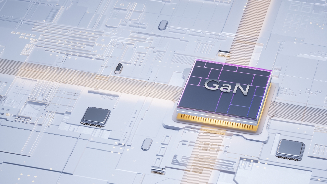
5-2. GaN (Gallium Nitride)
Characteristics
・Ultra-high-speed switching
・Low on-resistance
・Ideal for high-frequency operation
・Enables smaller, lighter devices
Applications
・USB fast chargers
・Data center power supplies
・Communications (RF)
・High-speed switching applications at low-to-medium voltage (up to around 650V)
GaN is the ace of high-speed, high-efficiency applications.
【6】General Power Device Structures (Vertical vs. Lateral)
Vertical structure
・Current flows vertically, from top to bottom.
・Well suited to high voltage tolerance and high current.
・Used in power MOSFETs, IGBTs, and SiC MOSFETs.
・Requires a larger substrate, but delivers very high performance.
Lateral structure
・Current flows horizontally, across the plane of the device.
・Well suited to high-speed switching and RF applications.
・Commonly used in GaN HEMTs.
・Easier to integrate with the substrate, making miniaturization easier.
【7】HEMT (High Electron Mobility Transistor)
A structure widely used in GaN devices.
Characteristics
・A heterostructure forms a “two-dimensional electron gas,” enabling ultra-high-speed switching.
・Low resistance and low losses.
・Widely used in RF communications (5G) and high-efficiency power supplies.
【8】Future Directions for Evolution
Outlook for SiC
・Mass production on 8-inch wafers (reducing costs)
・Lower on-resistance in SiC MOSFETs
・Accelerating research into 3D-structured SiC devices
Outlook for GaN
・Integration into power ICs (combining GaN with driver circuitry)
・Practical implementation of 900V-class GaN devices
・The rise of 3D (vertical) GaN structures
New materials
・Ga₂O₃ (gallium oxide) → for ultra-high voltage tolerance
・Diamond semiconductors → a candidate for the ultimate future material
【9】Summary
・Power devices are the “muscle” of the semiconductor world, handling large currents and high voltages.
・MOSFETs, IGBTs, and power diodes are the main device types.
・SiC and GaN are rapidly gaining adoption as ways to move beyond the limits of silicon.
・A clear division of roles is emerging: SiC for high voltage tolerance, GaN for high speed and low voltage.
・Continued market growth is all but certain across automotive, industrial, and energy applications.
Comprehension Check
1.In what kinds of applications are SiC and GaN each used?
2.What are the characteristics of the IGBT?
3.What is the mainstream structure used in power MOSFETs?
Column Supervisor: Koji Kakumoto (Otis Group Co., Ltd.)
After studying abroad and working in planning and development at a trading company, he joined Otis Group Co., Ltd. in 2011. While primarily working in the Corporate Planning Department, he has also served concurrently in manufacturing and technical divisions, and since 2018 has served as Representative Director, working to drive business growth and strengthen the organization.
This article is a general technical explanation intended for educational purposes and does not refer to any specific company, product, or technology.