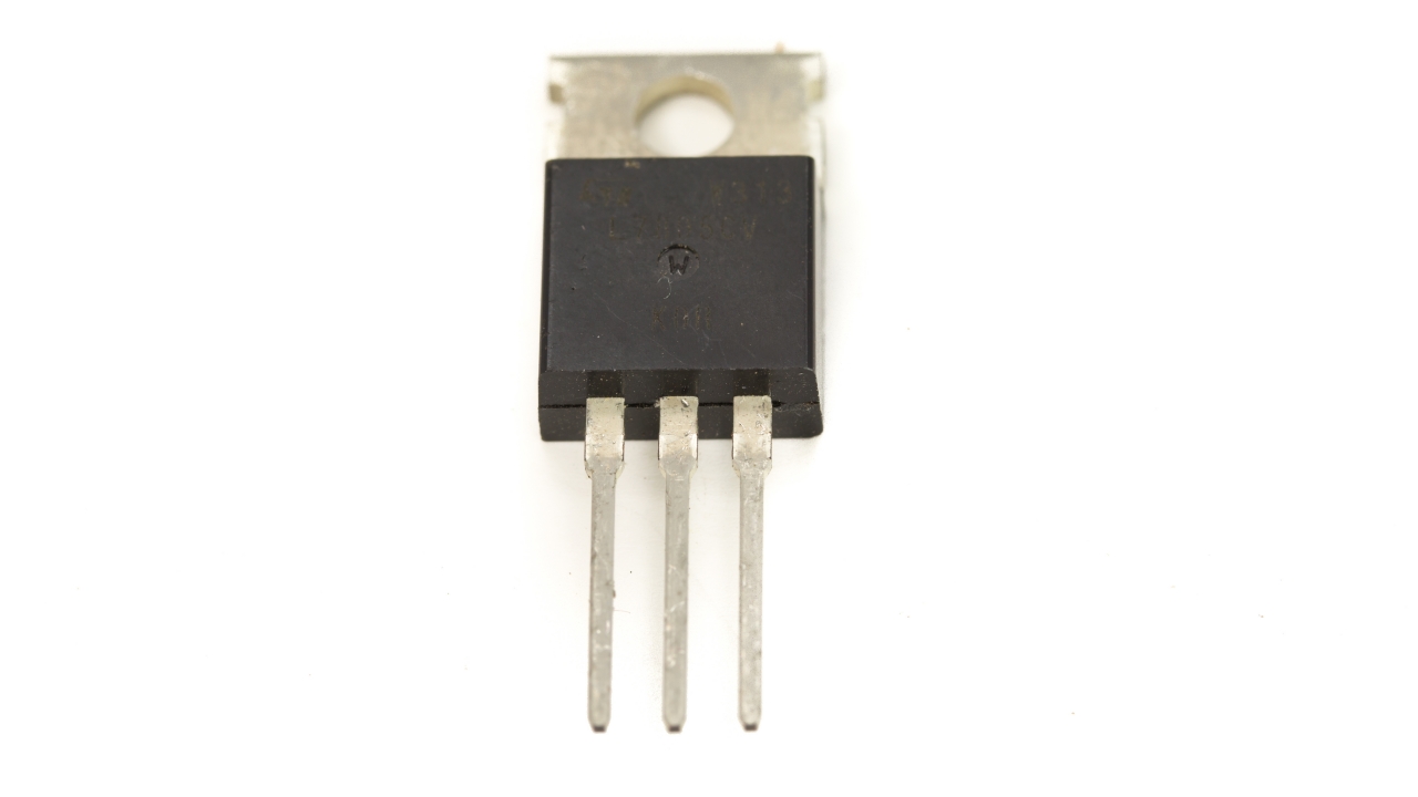
【1】Introduction
The MOSFET sits at the center of today’s semiconductor devices, used in nearly every type of electronics — CPUs, memory, smartphones, power ICs, sensors, and more.
The defining feature of the MOSFET is that it controls current using voltage. Whereas the BJT is a current-controlled device, the MOSFET is a voltage-controlled transistor. This mechanism enables low power consumption and high-speed, high-density integration.
【2】Overview of the Structure
A MOSFET is made up of four main parts:
1.Source: The terminal from which electrons or holes flow out.
2.Drain: The terminal into which electrons or holes flow.
3.Gate: The terminal that controls current using an electric field.
4.Substrate (or Body): The base layer of semiconductor material.
An insulating layer — an oxide film of SiO₂ — sits above the gate, and an electric field is formed through a metal electrode. This structure, Metal-Oxide-Semiconductor, is where the device gets its name.
【3】Operating Principle of an N-Channel MOSFET (Example)
Let’s look at how the N-channel MOSFET (NMOS), a representative type of MOSFET, operates.
1.The source and drain are N-type, while the substrate is P-type semiconductor material.
2.Normally, no electrons flow between the source and drain (the OFF state).
3.When a positive voltage is applied to the gate, electrons are drawn toward the surface of the P-type region, forming a conductive layer known as the channel.
4.Electrons then flow from the source to the drain through this channel.
In this way, a MOSFET turns current ON or OFF by controlling whether or not this channel forms, based on the gate voltage.
【4】Threshold Voltage (Vth)
In a MOSFET, the channel does not form until the gate voltage exceeds a certain level, known as the threshold voltage (Vth).
・Vg < Vth → No channel forms (OFF state)
・Vg > Vth → A channel forms (ON state)
This property makes the MOSFET ideal for use as a switch in digital circuits.
【5】Operation of a P-Channel MOSFET
The P-channel MOSFET (PMOS) has a structure opposite to that of the N-channel type:
・The source and drain are P-type, while the substrate is N-type semiconductor material.
・Applying a negative voltage to the gate forms a channel, allowing current to flow.
While NMOS conducts current via electrons, PMOS conducts current via holes. In CMOS circuits, these two types are used together as a pair.
【6】MOSFET Operating Regions
Depending on the relationship between the drain voltage and gate voltage, a MOSFET operates in one of three regions:
・Cutoff region: Vg < Vth → No channel forms, and current is zero.
・Linear region (triode region): Vg > Vth and Vd is low → Current increases proportionally, behaving like a resistor.
・Saturation region: Vg > Vth and Vd is high → Current becomes constant, and the device performs amplification.
Digital applications make use of the cutoff and saturation states, while analog applications operate the device within the linear region.
【7】Differences from the BJT (Comparison)
The key differences between the BJT and MOSFET are as follows:
・Control method: BJTs are current-controlled; MOSFETs are voltage-controlled.
・Input impedance: MOSFETs have very high input impedance, resulting in low power loss.
・Switching speed: MOSFETs are faster.
・Structure: BJTs consist of two PN junctions; MOSFETs use an insulated gate structure.
Because of these differences, BJTs are typically used for analog amplification, while MOSFETs are used in digital circuits and power switching applications.
【8】Advantages of the MOSFET
・Low power consumption (input current is essentially zero)
・Well suited to high-density integration, enabling smaller and denser devices
・High-speed switching
・Complementary operation is possible in a CMOS structure (NMOS + PMOS)
For these reasons, the MOSFET is often described as the heart of the integrated circuit.
【9】Drawbacks and Challenges
・Vulnerable to electrostatic discharge, which can damage the gate oxide layer.
・Large variation in threshold voltage can lead to malfunctions.
・As devices shrink, leakage current and short-channel effects become increasingly problematic.
To address these challenges, structures such as FinFET and GAA (Gate-All-Around) have been developed.
【10】Representative Applications
・Logic circuits in CPUs and GPUs
・Memory cells (SRAM, DRAM)
・Power circuits and motor drivers
・Analog circuits such as operational amplifiers
・Sensor circuits and communication modules
The MOSFET is a versatile component capable of handling amplification, switching, power control, and signal processing all at once.
【11】Summary
・A MOSFET is a transistor that controls current using voltage.
・The channel forms in response to the gate voltage, enabling ON/OFF control.
・Its defining strengths are high input impedance, low power consumption, and fast response.
・The MOSFET is a fundamental building block of modern ICs, LSIs, and VLSIs.
Comprehension Check
1.What does it mean for a MOSFET to be “voltage-controlled”?
2.Name the four terminals of a MOSFET.
3.What is the difference between an N-channel and a P-channel MOSFET?
Column Supervisor: Koji Kakumoto (Otis Group Co., Ltd.)
After studying abroad and working in planning and development at a trading company, he joined Otis Group Co., Ltd. in 2011. While primarily working in the Corporate Planning Department, he has also served concurrently in manufacturing and technical divisions, and since 2018 has served as Representative Director, working to drive business growth and strengthen the organization.
This article is a general technical explanation intended for educational purposes and does not refer to any specific company, product, or technology.