【1】Introduction
The MOSFET has served as the central technology of the semiconductor industry for decades, but as devices continued to shrink, its limits began to come into view.
The key problems included:
・Increasing leakage current
・Declining gate control ability (short-channel effects)
・Growing performance variation and localized heat concentration
Three-dimensional transistor structures emerged to address these challenges. The leading examples are FinFET and its successor, the GAA (Gate-All-Around) structure.
【2】The Structure of FinFET (Fin-Shaped Transistor)
FinFET is a three-dimensional device structure that replaced the traditional planar MOSFET. As its name suggests, it features a tall, narrow silicon structure resembling a fish’s fin.
Its distinctive structural features include:
・A channel region shaped as a vertically standing fin
・A gate arranged to wrap around three sides of the fin (a tri-gate structure)
・Stronger electric field control, significantly reducing leakage current
【3】How FinFET Works
In a traditional MOSFET, the gate could only control the top surface of the channel. In FinFET, the gate covers the channel from three directions — the top and both sides — enabling three-dimensional control over the flow of electrons.
This provides the following benefits:
・Suppresses threshold voltage variation caused by channel shortening
・Improves ON current (Ion)
・Reduces OFF current (Ioff)
・Maintains stable characteristics even at nodes below 10nm
【4】The Background Behind FinFET and Its Impact
FinFET became commercially viable after Intel began mass production at the 22nm node in 2011. TSMC, Samsung, and others subsequently adopted the technology as well, and it remains the mainstream structure today.
Advantages of FinFET:
・High gate control ability (high ON current, low OFF current)
・Low leakage current even at smaller process nodes
・Enables both high-speed operation and low power consumption
Disadvantages of FinFET:
・A complex manufacturing process
・Variation in fin shape can affect performance
・Achieving uniform fin height is difficult
【5】The Emergence of GAA (Gate-All-Around) Structures
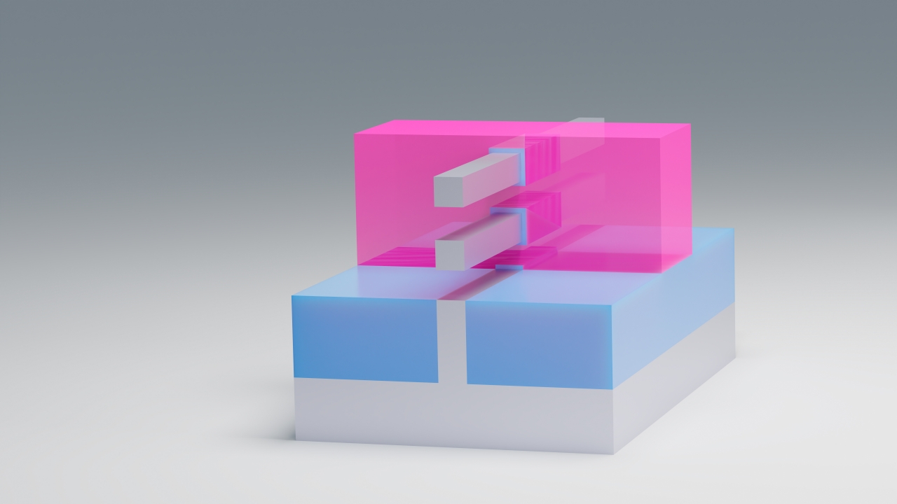
The GAA structure represents a further evolution. Where FinFET’s gate wraps around three sides of the channel, GAA extends this concept to fully surround the channel on all sides.
Structural features:
・The channel takes the form of a nanowire (a thin rod shape) or a nanosheet (a thin, flat sheet)
・The gate fully surrounds the channel, covering all 360 degrees
・Channel control is maximized, minimizing leakage
【6】Advantages of the GAA Structure
GAA delivers the following performance improvements:
・Further improved gate control, minimizing electrical interference
・Extremely low OFF current, enabling ultra-low power consumption
・Channel width (nanosheet thickness) can be adjusted to fine-tune device characteristics
・Extends the limits of miniaturization down to below 2nm
For these reasons, GAA is drawing attention as the mainstream technology of the post-FinFET era.
【7】Representative GAA Architectures
Different semiconductor manufacturers use different names and implementations for their GAA technology:
・Samsung: MBCFET (Multi-Bridge Channel FET)
・TSMC: Nanosheet GAA
・Intel: RibbonFET
・IBM / IMEC: Horizontal Nanowire GAA
While the naming differs, all share the same basic principle: fully surrounding the channel with the gate.
【8】Comparing FinFET and GAA
・Structure: FinFET uses a three-sided gate; GAA uses a fully surrounding gate.
・Control: GAA offers superior control, achieving 100% electric field coverage.
・Leakage current: GAA produces less leakage.
・Manufacturing difficulty: GAA is more difficult to manufacture and requires more process steps.
・Node applicability: FinFET is used from the 10nm to 5nm nodes; GAA is used from the 3nm node onward.
【9】Future Outlook
Research is already underway into structures that could succeed GAA:
・CFET (Complementary FET): A structure in which NMOS and PMOS are stacked vertically, enabling even greater density.
・2D semiconductor GAA: A GAA structure built from atomically thin layered materials such as MoS₂, enabling extreme miniaturization.
・Quantum dot transistors: Ultimate nanoscale devices that operate based on quantum effects in electrons.
Going forward, innovation is expected to advance along three fronts simultaneously: structure, materials, and physical phenomena.
【10】Summary
・FinFET is a 3D MOSFET structure that broke through the earlier limits of miniaturization.
・GAA takes this evolution further, controlling the channel from every direction.
・The industry is progressing through a clear evolutionary path: FinFET → GAA → CFET.
・As miniaturization continues, the fusion of structural and materials technology will be the key to further progress.
Comprehension Check (3 Questions)
1.What is the biggest difference between FinFET and a traditional MOSFET?
2.What are the advantages of the GAA structure?
3.What structure is drawing attention as a successor to FinFET?
Column Supervisor: Koji Kakumoto (Otis Group Co., Ltd.)
After studying abroad and working in planning and development at a trading company, he joined Otis Group Co., Ltd. in 2011. While primarily working in the Corporate Planning Department, he has also served concurrently in manufacturing and technical divisions, and since 2018 has served as Representative Director, working to drive business growth and strengthen the organization.
This article is a general technical explanation intended for educational purposes and does not refer to any specific company, product, or technology.