【1】What Is CMP?
CMP (Chemical Mechanical Polishing) is a process that combines a chemical reaction with mechanical polishing to flatten the surface of a wafer.
In modern semiconductor manufacturing, this flattening step is critically important, directly influencing wiring precision, yield, speed, and reliability.
【2】Why CMP Is Necessary
A semiconductor is built up from many stacked layers:
・Transistor layers
・Insulating layers
・Wiring layers (often ten or more)
・Additional insulating layers above them
As these layers accumulate, the surface becomes increasingly uneven.
If this unevenness is left uncorrected, it can cause:
・Focus problems during lithography
・Reduced etching precision
・Variation in wiring width and resistance
・Increased reliability failures
For this reason, each layer must be returned to a perfectly flat state before the next layer can be built — and that is exactly what CMP achieves.
【3】The Basic Mechanism of CMP
CMP is built around three key elements:
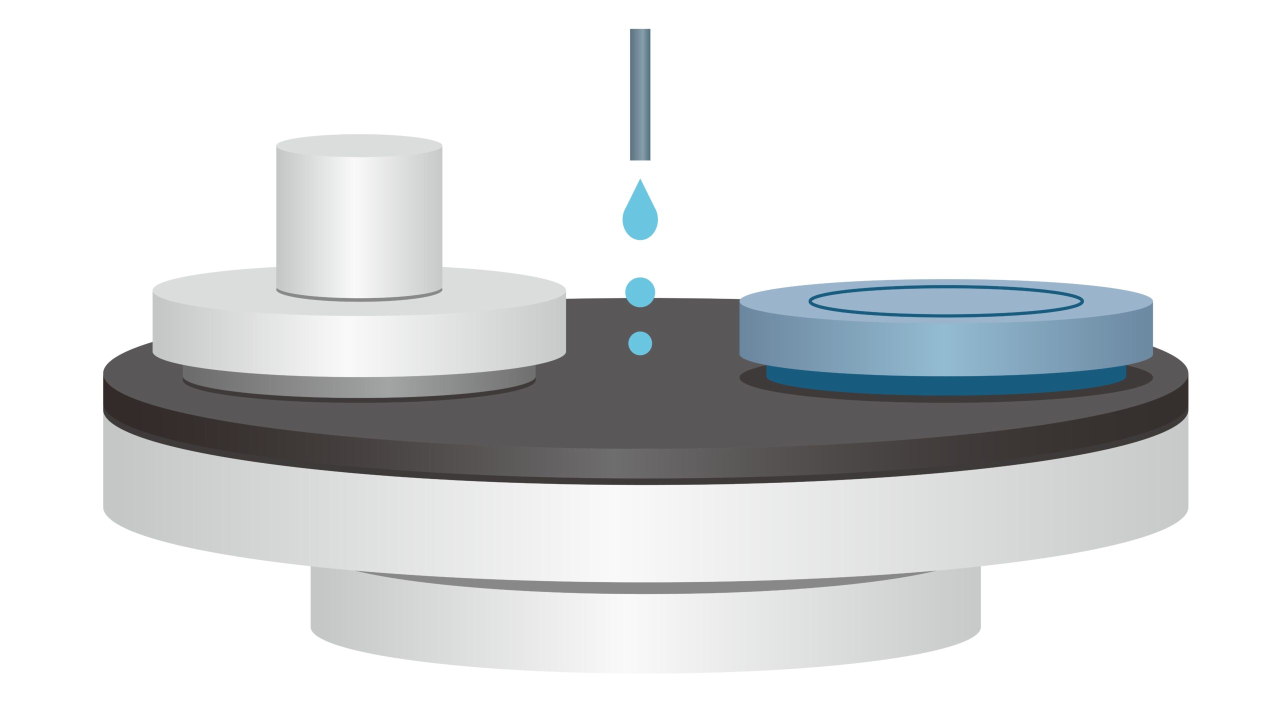
(1) Slurry
A mixture of chemical agents and abrasive particles (such as alumina or silica).
・The chemical reaction softens the film.
・The abrasive particles physically remove material.
This combination of chemistry and mechanics is the defining feature of CMP.
(2) Pad (polishing cloth)
A consumable component that presses against the wafer to polish it.
・Its hardness and surface structure affect polishing performance.
・Requires regular conditioning to maintain performance.
(3) Pressure and rotation (polishing)
The wafer and pad are rotated against each other while pressure is applied, achieving uniform material removal.
【4】Applications of CMP
CMP is used throughout virtually every stage of semiconductor manufacturing.
(1) STI (Shallow Trench Isolation)
After shallow trenches are filled with an oxide film, the excess material is removed and the surface flattened.
(2) Gate formation (metal gate CMP)
After the gate stack is formed, excess material is removed.
(3) Multilayer copper wiring
Because copper wiring is formed using the damascene method, CMP is essential:
・Cu CMP
・Barrier film (Ta/TaN) CMP
・ILD (insulating layer) CMP
CMP also plays a role in reducing resistivity and controlling surface roughness.
【5】Key Performance Indicators (KPIs) for CMP
Because both over-polishing and under-polishing can be critical failures, CMP requires extremely fine-grained control.
Representative KPIs include:
・Removal rate: the speed at which material is removed
・Uniformity: variation in polishing across the wafer
・Scratch defects: polishing-induced scratches
・Dishing: a phenomenon where copper alone becomes recessed
・Erosion: a phenomenon where the surrounding insulating layer is also worn away and recessed
・Residue: leftover film that should have been removed
Dishing and erosion, in particular, can increase wiring resistance and degrade device reliability.
【6】The Relationship Between the Damascene Process and CMP
Copper wiring is formed using the damascene method, which follows these steps:
1.Trenches are etched into an insulating layer.
2.A barrier film and copper are deposited across the entire surface.
3.CMP removes the copper everywhere except within the trenches, leaving only the wiring behind.
In other words, the relationship between copper wiring and CMP is so close that it could almost be said that copper wiring is created by CMP.
Modern multilayer wiring simply could not exist without CMP.
【7】The Challenges of CMP and Process Control
CMP is considered a difficult process for several reasons:
・The complex interaction between chemical reactions and mechanical polishing
・Achieving uniform polishing across 3D structures
・Removal rates that vary depending on local wiring density (pattern density dependency)
・Slurry degradation and supply conditions
・Pad condition
・Local variation in pressure distribution across the wafer
As a result, CMP demands a combined mastery of materials science, mechanical control, fluid control, and process optimization.
【8】Recent Trends in CMP
The following technologies are central to CMP in today’s leading-edge processes:
・Monolayer polishing (precise removal of extremely thin layers)
・HF-free CMP slurries for copper rewiring
・Multilayer planarization CMP for 3D NAND
・AI-driven real-time process optimization
・Automated pad diagnostics (using image and acoustic analysis)
・Low-damage CMP (reduced-stress polishing)
Going forward, continued advancement is expected through the combination of materials, data, and AI.
【9】Summary
・CMP is a critical process for flattening the wafer surface.
・It combines a chemical reaction with mechanical polishing.
・It is used throughout nearly every step of manufacturing, including copper wiring and STI formation.
・Dishing and erosion are among the most significant challenges.
・CMP precision directly affects both yield and reliability.
・Ongoing advances in AI and sensing technology continue to drive its evolution.
Comprehension Check (3 Questions)
1.What is the purpose of CMP?
2.Name one representative application where CMP is essential.
3.Name one representative type of defect that can occur during CMP.
Column Supervisor: Koji Kakumoto (Otis Group Co., Ltd.)
After studying abroad and working in planning and development at a trading company, he joined Otis Group Co., Ltd. in 2011. While primarily working in the Corporate Planning Department, he has also served concurrently in manufacturing and technical divisions, and since 2018 has served as Representative Director, working to drive business growth and strengthen the organization.
This article is a general technical explanation intended for educational purposes and does not refer to any specific company, product, or technology.