【1】What Is Metallization?
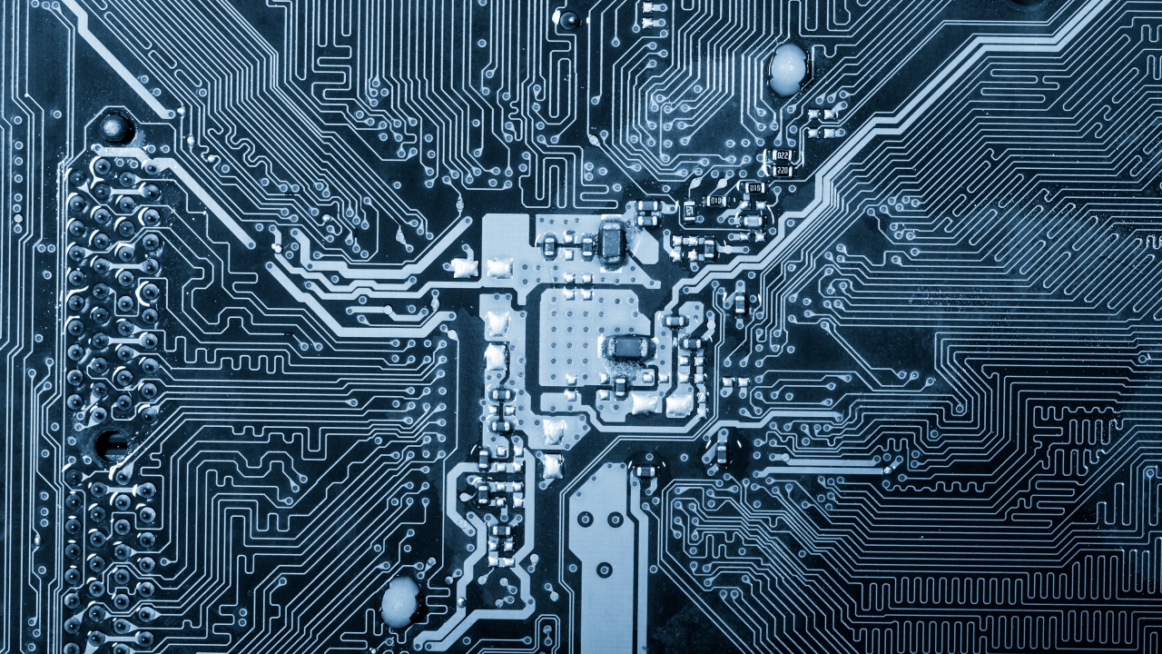
Metallization is the process of forming the metal wiring that electrically connects transistors to one another.
The performance of this wiring directly determines a chip’s:
・Operating speed
・Power consumption
・Reliability
・Heat generation
・Yield
Modern chips contain 10 to 15 or more layers of wiring, which means wiring technology has become one of the decisive factors in device performance.
【2】Types and Characteristics of Wiring Materials
(1) Al (Aluminum)
・Once the dominant material
・Highly reliable, but with relatively high resistivity
・Now largely limited to analog and power applications
(2) Cu (Copper)
・The dominant material in today’s logic devices
・Low resistance, enabling high speed
・However, it diffuses easily into silicon, making a barrier film essential
・Difficult to etch, so it must be formed using the damascene method
(3) Co / Ru (next-generation candidates)
Drawing attention as a way to avoid the rising resistance of copper wiring as it continues to shrink.
・Co: shows less increase in wiring resistance
・Ru: may allow for barrier-free wiring
【3】The Basic Wiring Formation Process
Copper wiring is formed using the “damascene method.”
Damascene process steps
1.An insulating film (low-k material) is deposited.
2.Trenches and vias (holes) are formed via etching.
3.A barrier film (such as TiN/TaN) is deposited.
4.A thin copper seed layer is deposited via sputtering.
5.Electrochemical plating (ECP) fills the trenches with copper.
6.CMP removes excess copper and flattens the surface.
7.The process moves on to the next layer, building up the multilayer structure.
Because copper cannot be etched using plasma, this process uses a distinctive approach: fill first, then remove the excess, rather than etching directly.
【4】The Role of the Barrier Film
The barrier film acts as a protective wall that prevents copper from diffusing into the surrounding material.
・Common materials include TiN, TaN, Co, and manganese-based compounds.
・These films, only a few nanometers thick, protect the underlying silicon.
・As devices shrink, these films must become both thinner and higher performing.
Because a thinner wiring width means the barrier film’s own thickness has an increasingly large impact on overall wiring resistance, developing barrier-free wiring is becoming a key priority for the future.
【5】Key Points of Copper Plating (ECP)
This is the process of growing copper through electrochemical plating.
・Copper is deposited electrochemically on top of the seed layer.
・Additives are used to control growth from the bottom upward.
・Early-stage defects, such as voids and seams, directly affect reliability.
Incomplete plating can lead to wiring breaks, which in turn cause reduced yield — a critical failure mode.
【6】The Structure of Multilayer Wiring (the Interconnect Stack)
Different wiring layers serve different roles:
・Lower layers (M0–M2): thin wiring for high-speed signals
・Middle layers (M3–M6): internal logic wiring
・Upper layers (M7 and above): thicker wiring for power lines and clock signals
This layered structure optimizes wiring resistance and capacitance throughout the chip.
【7】The RC Delay Problem (Wiring Resistance × Wiring Capacitance)
The greatest enemy of wiring miniaturization is RC delay.
・As wiring becomes thinner, resistance (R) increases.
・As wiring lines move closer together, capacitance (C) increases.
The result: this becomes the single largest factor limiting circuit speed.
Countermeasures include:
・Low-k films (insulating materials with a low dielectric constant)
・Thinner barrier films
・Alternative metals (Co, Ru)
・Air-gap structures (using air itself to lower the dielectric constant)
【8】Challenges Becoming Apparent at the 3nm/2nm Nodes
・A sharp rise in copper’s resistance due to size effects
・Barrier films becoming relatively too thick
・High aspect-ratio vias that are difficult to fill completely
・Reduced reliability due to the brittleness of low-k films
・Dishing and erosion caused by CMP
・Increased heat generation from densely packed wiring
This is precisely why it’s often said that wiring, more than the transistor itself, is now approaching its limits.
【9】Recent Trends
The following developments are drawing attention in next-generation wiring:
・Barrier-free ruthenium wiring (offering lower resistance and a simpler process)
・Mass production of cobalt wiring, particularly for vias
・Air-gap insulating structures
・3D wiring enabled by hybrid bonding
・AI-driven optimization of CMP and wiring design
・Low-temperature wiring for quantum computing applications
The key themes are lower resistance, higher reliability, and 3D integration.
【10】Summary
・Wiring formation is one of the final determining factors in overall semiconductor performance.
・Copper wiring requires the damascene method.
・The barrier film has become a major challenge as devices continue to shrink.
・RC delay is what ultimately governs circuit speed.
・New materials such as Co and Ru are the key to the next generation of wiring.
・Wiring technology has become the single biggest bottleneck at the 2nm node.
Comprehension Check (3 Questions)
1.Why can copper wiring only be formed using the damascene method?
2.Explain the role of the barrier film (TiN/TaN).
3.Why does wiring resistance increase as devices shrink?
Column Supervisor: Koji Kakumoto (Otis Group Co., Ltd.)
After studying abroad and working in planning and development at a trading company, he joined Otis Group Co., Ltd. in 2011. While primarily working in the Corporate Planning Department, he has also served concurrently in manufacturing and technical divisions, and since 2018 has served as Representative Director, working to drive business growth and strengthen the organization.
This article is a general technical explanation intended for educational purposes and does not refer to any specific company, product, or technology.