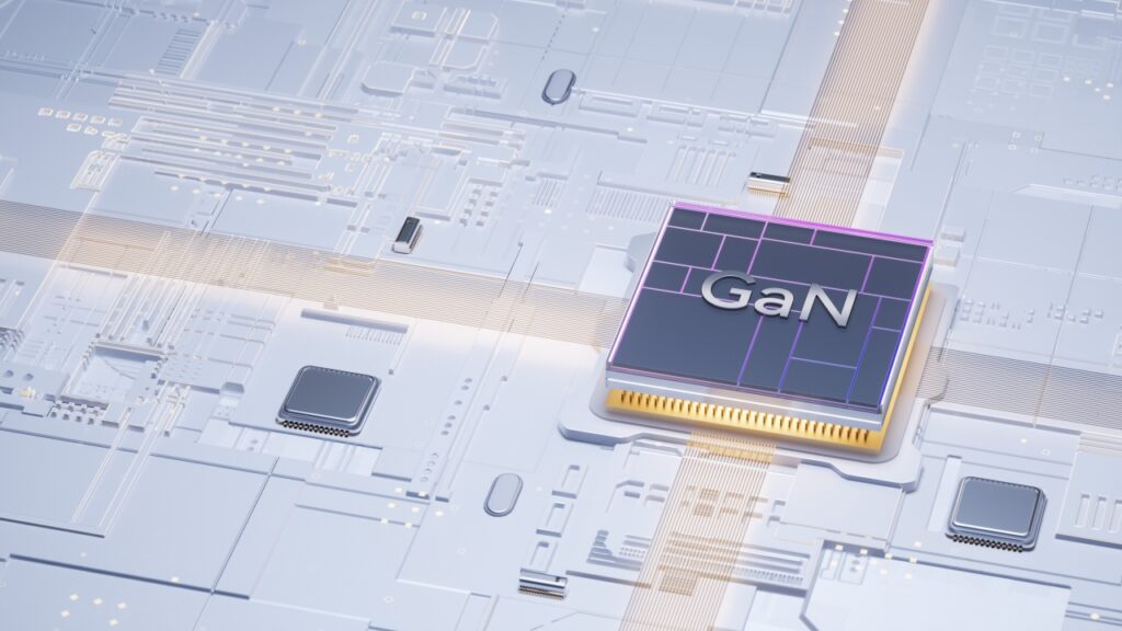
【1】Why Are SiC and GaN Attracting Attention?
Demand is surging for devices that can withstand high-voltage, high-current, and high-temperature environments, such as in electric vehicles (EVs), renewable energy, servers, and fast chargers.
To go beyond the limits of Si, wide-bandgap (WBG) materials have taken center stage.
Representative examples:
● SiC (silicon carbide): high voltage × high temperature × high reliability
● GaN (gallium nitride): high frequency × high efficiency
Because they exceed the physical limits of Si, they offer the following strengths:
● Large bandgap
● High thermal conductivity (SiC)
● High breakdown field strength
● Capable of high-temperature operation
● Low-loss switching
As a result, they contribute directly to energy savings across society, such as improving EV energy efficiency and reducing data center power consumption.
【2】Manufacturing Process Challenges Specific to SiC Devices
Compared with Si, SiC is a material that is “very difficult to process.”
(1) Wafer Quality Challenges
SiC crystals have many defects.
・BPD (Basal Plane Dislocation)
・TED (Threading Edge Dislocation)
・Micropipes, etc.
These directly affect yield and electrical characteristics.
(2) Etching Is Difficult
Because SiC is hard and chemically unreactive, high-power plasma must be used.
Challenges:
・Low etching rate
・Thicker damage layer
・Difficult to improve surface roughness
・Difficult to ensure uniformity
(3) Heat Treatment (Annealing) at High Temperatures
The activation annealing temperature is 1,500°C or higher—extremely high.
Selecting equipment, managing substrate stress, and choosing materials are difficult.
(4) Gate Insulating Film (SiO₂) Quality Is Worse Than on Si
The interface defect density (Dit) is high, making the threshold voltage difficult to stabilize.
→ This remains a major research challenge today.
【3】Process Challenges Specific to GaN Devices
GaN excels in high-speed, high-frequency applications, but it has difficulties different from those of SiC.
(1) Substrate Selection Is Difficult
Because single-crystal GaN is expensive, most commercial products are grown on dissimilar materials, such as:
・GaN on Si
・GaN on SiC
・GaN on Sapphire
As a result, the following tend to occur:
・Warpage due to differences in thermal expansion coefficients
・Cracks during deposition
・More crystal defects
(2) Increasingly Complex HEMT Structures
The mainstream GaN device is the HEMT (High Electron Mobility Transistor).
Key elements:
・Composition and thickness of the AlGaN layer
・2DEG (high-mobility electron layer)
・p-GaN gate (for normally-off operation)
Challenges:
・Gate breakdown voltage
・Trade-offs with RF characteristics
・Surface traps (current instability)
(3) Interface Cleaning and Surface Control Are Difficult
Inadequate pretreatment significantly reduces yield.
【4】Manufacturing Difficulties Common to SiC and GaN
Compared with Si, both are “difficult to achieve good yields with.”
Reasons:
・Many crystal defects
・Low material homogeneity
・Narrow process window
・High material stress from heat treatment and other steps
・Difficult to balance design and process
For this reason, they are comprehensive devices that require processing technology, equipment, and material understanding all together.
【5】Representative Device Structures and Processes
(1) SiC MOSFET
・Trench types are mainstream
・Gate oxide reliability is key
・On-resistance is reduced by optimizing the source cells
(2) GaN HEMT
・The 2DEG at the AlGaN/GaN interface carries the current
・Normally-off operation through a p-GaN gate
・Gate leakage suppressed with an MIS structure
(3) Methods for Achieving High Breakdown Voltage
・Higher-quality drift layers
・Optimized edge termination structures
・Designs that make the electric field distribution uniform
【6】Reliability and Yield Challenges
Main Challenges for SiC
・Degradation of the gate insulating film
・Leakage and breakdown caused by crystal defects
・Parameter shifts during high-temperature operation
Main Challenges for GaN
・Gate breakdown voltage
・Current spikes caused by surface traps
・Thermal runaway during RF operation
Common Challenges
・High manufacturing costs
・Low yields keep product prices high
This is also a field in which Japanese manufacturers are strong, and the know-how to achieve high reliability is a key differentiator.
【7】Latest Trends and Future Directions
Volume production of 8-inch SiC wafers
→ Cost improvements are progressing
Accelerated research on vertical GaN
→ Combines high breakdown voltage with high speed
Improvements in MOS / MIS structures
The triple requirement of high voltage × high frequency × low loss
→ Demand is surging in EVs, data centers, and renewable energy
Optimization together with packaging
→ For SiC/GaN, thermal design, parasitics, and mounting directly affect performance
【8】Summary
・SiC/GaN are WBG materials with properties that surpass Si
・They are technologies that will transform social infrastructure such as EVs, renewable energy, and servers
・However, manufacturing is extremely difficult, and securing yield is the biggest challenge
・SiC is hard, making processing and heat treatment difficult
・GaN faces challenges with dissimilar substrates and surface traps
・Ensuring reliability determines competitiveness
・Going forward, vertical GaN and 8-inch SiC will be game changers
Comprehension Check
1.Why are SiC and GaN, rather than Si, used for high-voltage applications?
2.Why is etching SiC devices particularly difficult?
3.Why is the 2DEG important in GaN HEMTs?
Column Supervisor: Koji Kakumoto (President, OTIS Co., Ltd.)
After studying abroad and working in planning and development at a trading company, he joined OTIS Co., Ltd. in 2011. While primarily working in the Corporate Planning Department, he has also served concurrently in manufacturing and technical divisions, and since 2018 has served as President, working to drive business growth and strengthen the organization.
This article is a general technical explanation intended for educational purposes and does not refer to any specific company, product, or technology.