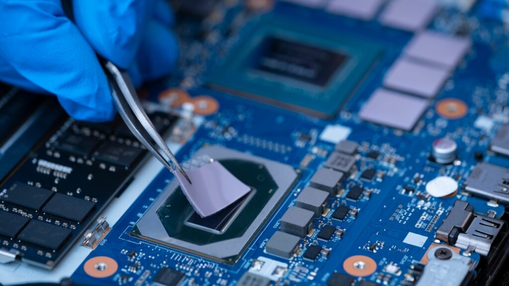
For example, in AI servers, thermal design can become a problem even before chip performance.
The higher the density, the greater the amount of heat generated, and how that heat is dissipated determines system performance.
In environments where many chips of several hundred watts are lined up, cooling design itself can become a performance constraint.
The evolution of semiconductors has always been a battle against heat.
In addition, the higher signal speeds become, the more electromagnetic noise (EMI) and signal interference become major challenges.
In high-speed communication in the GHz band and beyond, the dielectric constant, conductivity, and shape precision of materials affect signal quality.
It is not unusual for slight differences in shape or material properties to determine communication quality and reliability.
Furthermore, as semiconductor packaging becomes more advanced, material structures become extremely complex.
Thin films, adhesive layers, metal foils, insulating materials, and more are combined, sometimes into multilayer structures of dozens to hundreds of layers.
In such structures, differences in thermal expansion between materials, stress, humidity, temperature changes, and other factors affect long-term reliability, so materials design and structural design become important.
In other words, in the future semiconductor society, technologies such as the following will support society in inconspicuous ways.
・Material selection
・Microfabrication
・Precision lamination
・Thermal countermeasures
・EMI countermeasures
・Reliability design
These technologies are not flashy. In reality, however, they are the very foundation of the semiconductor industry.
Even the most advanced chips cannot become products without the right materials and processing technologies.
What has been attracting particular attention in recent years is the shifting boundaries between processing technologies.
Today, in semiconductor-related microfabrication, processes such as laser processing and etching are often considered mainstream.
In recent years, however, the precision of mechanical processing technologies such as die machining and precision pressing has also been improving rapidly.
Especially for thin materials such as films and metal foils, the boundaries between processing technologies such as
・Laser processing
・Etching
・Precision press processing
are gradually drawing closer.
Traditionally, in areas requiring processing precision from tens of microns down to the submicron level, chemical etching and laser processing have often been chosen.
In recent years, however, thanks to advances in
・High-precision dies
・Positioning control precision of processing machines
・Understanding of material behavior
・Continuous processing
areas where mechanical processing is approaching the same level have begun to appear.
If this trend continues, the roles of processing technologies such as
laser,
etching,
and precision pressing
may be redefined in the future.
Depending on the application, mechanical processing may become a new option in areas where it has not been considered until now.
The semiconductor industry may look like a world of advanced electronic technology.
However, at its foundation there have always been advances in materials and processing.
And the very moment when the boundaries between processing technologies change is also the point at which new industrial structures are born.
This structure will not change in the future semiconductor society either.
On the contrary, the more advanced chips become, the more important peripheral materials and processing technologies will be.
It is the technologies supporting things from unseen places that form the foundation of the semiconductor industry.
Summary
・Semiconductor performance is not determined by circuit design alone
・Thermal design, EMI countermeasures, and material structures determine system performance
・As packaging becomes more advanced, the importance of materials and processing is increasing
・The boundaries between laser, etching, and precision press processing are shifting
・Even in the future semiconductor society, “invisible technologies” will support the industry
This concludes our study of semiconductors.
Thank you very much for staying with us for so long.
The word “semiconductor” may sound difficult, but in essence it is a collection of materials, processing, and accumulated technologies.
And the society of the future will be supported not only by AI and computers but also by such invisible technologies.
If, through this series, you have come to think that “the world of semiconductors is interesting” or “I got a small sense of the depth of manufacturing,” we would be very happy.
The world of technology is evolving every day.
Society will continue to change greatly through new materials, new processing technologies, and new ideas.
We hope to continue enjoying these changes together with you.
It is not only cutting-edge chips that support the future of semiconductors.
It is the materials and processing technologies that support them behind the scenes that will shape the society of the future.
We at OTIS want to continue to be a company that supports such industries with our technology.
Column Supervisor: Koji Kakumoto (President, OTIS Co., Ltd.)
After studying abroad and working in planning and development at a trading company, he joined OTIS Co., Ltd. in 2011. While primarily working in the Corporate Planning Department, he has also served concurrently in manufacturing and technical divisions, and since 2018 has served as President, working to drive business growth and strengthen the organization.
This article is a general technical explanation intended for educational purposes and does not refer to any specific company, product, or technology.