What Is a Semiconductor? ― The Differences Between Conductors, Insulators, and Semiconductors
Materials are divided into three types according to how easily they conduct electricity.
Conductors that conduct electricity well (copper, aluminum, etc.), insulators that hardly conduct it at all (glass, rubber, etc.), and semiconductors that sit between the two.
The greatest characteristic of semiconductors is that their conductivity changes depending on external conditions such as temperature, light, and voltage. This property of being “a material that responds according to conditions” is the basis of all switches, sensors, and computing elements. No electronic device in modern society could exist without this property.
Why Silicon Takes the Lead ― Doping and How Electrons and Holes Work
There are three reasons why silicon (Si) is overwhelmingly mainstream among semiconductor materials: it is abundant and inexpensive on Earth, its crystal structure is stable and suited to precision processing, and an oxide film (SiO₂) can be formed within it and used as an insulating layer. As a material that combines ease of handling with high performance, it still reigns at the center of the semiconductor industry today.
The flow of electricity in a semiconductor arises from the movement of two types of carriers: electrons (negative) and holes (vacancies left by electrons, positive). Through doping, in which tiny amounts of impurities are added, it is possible to create N-type semiconductors rich in electrons and P-type semiconductors rich in holes, and this is the starting point for all devices. Semiconductors are now called “the rice of industry” and have become strategic materials that determine a nation’s technological strength, economic power, and security.
Types of Semiconductor Materials ― Elemental and Compound Semiconductors
Semiconductor materials are broadly divided into two types: elemental semiconductors and compound semiconductors. Elemental semiconductors, represented by silicon and germanium, are inexpensive and well suited to mass production, and they are used as the mainstream materials for logic ICs and memory. Compound semiconductors, on the other hand, combine two or more elements, have properties that cannot be achieved with silicon, and are selected according to the application.
Si (Silicon)
General-purpose and inexpensive. The mainstream material for logic and memory
Ge (Germanium)
High electron mobility. Suited to high-speed operation and infrared sensor applications
GaAs (Gallium Arsenide)
High frequency and high speed. Strong in 5G communications, satellite, and space applications
InP (Indium Phosphide)
Used in optical communications and laser diodes. The mainstay of high-speed optical devices
The Rise of Next-Generation Materials ― How SiC, GaN, and Graphene Are Changing Industry
To go beyond the performance limits of silicon, new-generation materials called wide-bandgap semiconductors are spreading rapidly. The wider the bandgap, the higher the withstand voltage, the higher the operating temperature, and the lower the losses that can be achieved, making them indispensable materials for realizing a decarbonized society, including EVs, 5G, and renewable energy.
● SiC (silicon carbide): High withstand voltage and high-temperature capability. Its adoption as a power semiconductor for EV inverters is expanding rapidly
● GaN (gallium nitride): Excellent for high-speed switching and miniaturization. Standardization is advancing in fast chargers and 5G base stations
● Ga₂O₃ (gallium oxide): Research is under way on it as a next-generation power semiconductor material with withstand-voltage characteristics exceeding those of SiC
● Graphene and 2D materials: Ultra-thin materials consisting of a single layer of carbon atoms. With extremely high electron mobility, they are attracting attention as post-silicon materials
The Evolution of Devices ― From PN Junctions to GAA Chips
The PN junction, which joins N-type and P-type semiconductors, is the starting point of everything. It developed into diodes, which let current flow in only one direction, and MOSFETs, which control and amplify current, and the CMOS structure, which combines N-type and P-type devices, became the standard for digital circuits by keeping static power consumption close to zero.
PN junction → Diode → MOSFET → CMOS → FinFET → GAA
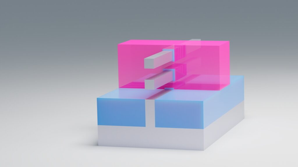
To deal with the limits of scaling, FinFET, with its three-dimensional gate structure, has become essential from 22nm onward, and GAA (Gate-All-Around), in which the gate controls the channel from all sides, from 2nm onward. On a chip, components for different purposes are integrated, such as SRAM for high-speed cache, high-capacity DRAM, non-volatile flash memory, the CPU for general-purpose computing, and the GPU for massively parallel processing.
Key Points of This Column
● Semiconductors are materials “whose conductivity changes with conditions,” sitting between conductors and insulators
● Silicon is mainstream for three reasons: low cost, stability, and the ability to form an oxide film. Doping is the basis of everything
● Materials are broadly divided into elemental and compound semiconductors. Choosing them according to the application determines performance
● Wide-bandgap materials such as SiC and GaN are transforming the EV, 5G, and renewable energy industries
● Devices have evolved from PN junctions → MOSFET → CMOS → FinFET → GAA, breaking through the limits of scaling with structure
Supervised by: Koji Kakumoto (President, OTIS Co., Ltd.)
*This article integrates and summarizes the content of Chapters 1–3. For details, please refer to the original article for each chapter.