An Overview of the Manufacturing Process ― The Two-Stage Structure of Front-End and Back-End Processes
Semiconductor manufacturing is broadly divided into two stages: the front-end process and the back-end process. The front-end process forms transistors and wiring on the wafer: transistors and elements are created in FEOL (Front-End Of Line), and the elements are connected to one another with copper wiring in BEOL (Back-End Of Line). In the back-end process, the wafer is cut into individual chips (dicing), which are then encapsulated, assembled, and tested to become shippable products.
Wafer manufacturing → FEOL (element formation) → BEOL (wiring formation) → Dicing → Packaging and testing → Shipping
Leading-edge chips involve more than 1,000 process steps, and it takes several months to complete them all. Because a difference of a few percent in yield (the rate of good products) affects cost competitiveness by orders of magnitude, quality control at each step forms the core of manufacturing competitiveness.
The Core of the Front-End Process ― Lithography, Etching, and CMP Carve the Circuits
Each step of the front-end process makes full use of light, chemicals, heat, and ions to build structures with nanometer precision. Among them, lithography (exposure) is the core of scaling: because the fineness of patterns is determined by the wavelength of light, advances in light source technology define the generations of semiconductors.
Lithography (Exposure)
Transfers the photomask pattern onto the wafer. The most important process and the key to scaling
Etching
Removes unnecessary films with chemicals or plasma to form circuit patterns
Ion Implantation
A doping process that implants impurity ions to form N-type and P-type regions
CMP (Chemical Mechanical Polishing)
Planarizes the surface at the atomic level. Makes it possible to build up multilayer wiring
By repeating and stacking these processes, tens of billions of transistors are formed on a single wafer. Each process depends closely on the processes before and after it, and an error in one process affects the quality of the entire final product.
The Limits of Scaling and the Breakthroughs ― From FinFET to GAA, and the Role of EUV
A semiconductor’s “nm node” is a generation name: the smaller the number, the higher the performance, the lower the power consumption, and the higher the integration.
However, FinFET (a three-dimensional fin-shaped gate structure), which was mainstream from 7nm to 5nm, reaches its physical limits at 2nm and beyond, making a transition to GAA (Gate-All-Around), in which the gate controls the channel from all sides, essential.
● EUV lithography: Next-generation lithography equipment that uses extreme ultraviolet light with a wavelength of 13.5nm. An essential technology for advanced nodes, costing several tens of billions of yen per unit. Supplied exclusively by ASML
● High-NA EUV: An even more advanced generation of EUV with a higher numerical aperture. Under development as a technology to support scaling to 1.4nm and beyond
● GAA (nanosheet structure): The channel is made into thin sheets and controlled by the gate from all sides. Suppresses current leakage and enables further scaling
● TSMC, Samsung, and Intel: The three companies compete at advanced nodes, and fierce technological competition continues over volume production technology for 2nm and beyond
Chiplets and 2.5D/3D Integration ― A New Axis of Performance Improvement in Place of Scaling
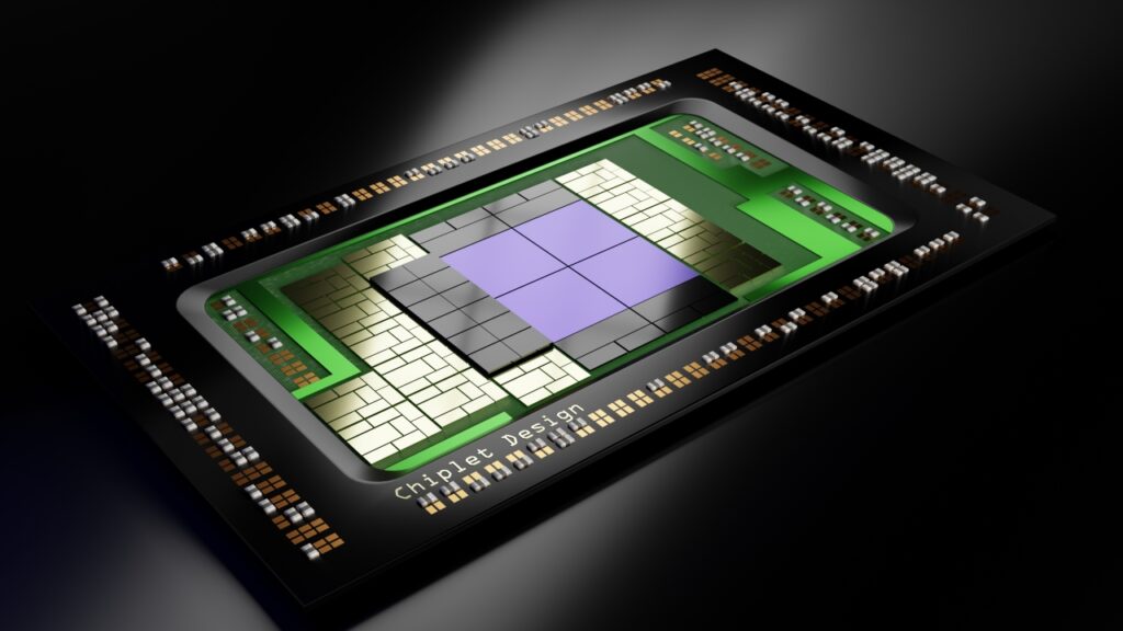
As performance improvements through scaling alone reach their limits, chiplet design, which combines chips divided by function, and 2.5D/3D integration, which integrates them at high density, have become the new main axes. Standardization of connection specifications (UCIe) is also advancing rapidly so that chips from different manufacturers can be freely combined.
● Chiplets: A large chip is divided by function, manufactured separately, and combined later. Enables better yield, lower costs, and mixing of different technologies
● 2.5D packaging (interposer): Multiple chips are placed side by side on a silicon or organic substrate (interposer). Adopted for connecting HBM memory and GPUs
● 3D packaging (stacking): Chips are stacked vertically and connected with TSVs. Maximizes bandwidth and minimizes latency
● Hybrid bonding: A solder-free direct Cu-Cu bonding technology. Enables ultra-high-density connections at µm pitches and below, and has become a key technology for 3D stacking
The Evolution of Packaging ― Becoming a Core Technology That Determines System Performance
Packaging is no longer a technology for “wrapping chips”; it has transformed into a core technology that determines system performance itself. It has evolved rapidly from conventional types such as DIP, QFP, and BGA to flip chip, fan-out, TSV stacking, and 3D integration, and the main battleground of performance competition for AI chips is now shifting to packaging technology.
● Fan-out WLP: Chips are embedded in mold resin and rewired. Achieves thinness, high density, and low cost at the same time. Widely adopted in smartphone SoCs
● HBM (High Bandwidth Memory): DRAM is stacked vertically with TSVs and connected to the GPU in 2.5D. Delivers the ultra-large capacity and ultra-high-speed bandwidth required for AI training
● Liquid cooling and optical I/O: As AI chip power consumption increases, air cooling is reaching its limits. Liquid-cooled packages and optical wiring (co-packaged optics) are being put into practical use
● Yield management: In multi-die configurations, good-product rates multiply. “Whether it can be manufactured stably in volume” rather than “whether it can be made” is the biggest axis of competition
Key Points of This Column
● Manufacturing consists of three stages: FEOL (element formation), BEOL (wiring formation), and the back-end process (packaging and testing)
● Lithography, etching, CMP, and ion implantation are the main front-end technologies. Lithography determines scaling
● From 2nm onward, the GAA structure is essential. Without EUV, advanced-node manufacturing is not possible
● Chiplets + 2.5D/3D integration have become the new main axis for “performance improvement in place of scaling”
● Packaging is a core technology that determines system performance. Yield management is the key to competitiveness
Supervised by: Koji Kakumoto (President, OTIS Co., Ltd.)
*This article integrates and summarizes the content of Chapters 4–6. For details, please refer to the original article for each chapter.