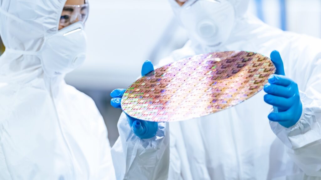
Inspection and Characterization Technology ― The Cornerstone of Quality Assurance That Catches Invisible Defects
In semiconductors made with nanometer precision, invisible defects determine product yield and reliability. Quality is ensured by two pillars: in-line inspection, carried out at each stage of manufacturing, and functional testing after completion.
● Optical inspection (AOI): High-speed 100% inspection for pattern defects and foreign particles. High throughput makes it the main method in the front-end process
● SEM (scanning electron microscope): Directly observes shapes and cross-sections with nanometer precision. Indispensable for analyzing the causes of defects
● Wafer probing: Checks electrical characteristics and operation in wafer form after the front-end process. Removes defective dies early
● Reliability and environmental testing: Tests that guarantee long-term durability, such as resistance to high temperature, humidity, vibration, and ESD
AI-based defect classification and yield analysis are spreading rapidly, and in-line SPC (statistical process control), which feeds inspection data back to manufacturing processes in real time, has become the key to competitiveness.
The Industry's Division of Labor ― The Ecosystem of Fabless Companies, Foundries, and OSATs
Semiconductors cannot be made by a single company. They depend on a complex division-of-labor structure (ecosystem) in which design, manufacturing, back-end processing, materials, and equipment work together. The industry has shifted from “vertical integration (IDM)” to “horizontal division of labor,” evolving into a structure in which each specialist hones its technology to the limit in its own field.
Design (fabless) → Front-end process (foundry) → Back-end process (OSAT) → Assembly and shipping
Fabless
Specialize in design without owning factories. NVIDIA, Qualcomm, and AMD are representative
Foundry
Specialize in contract manufacturing for the front-end process. TSMC and Samsung lead the world
OSAT
Companies specializing in the back-end process (packaging and testing). ASE and Amkor are the major players
IDM
Handle everything from design to manufacturing and sales in-house. Intel, Samsung, Toshiba, and others fall into this category
Supply Chain Risks and Restructuring ― The Foundation Supported by Equipment, Materials, and EDA
The semiconductor supply chain is supported not only by product manufacturers but also by manufacturing equipment makers, materials makers, and EDA (electronic design automation) tool vendors as an indispensable foundation. Concentration in specific companies and regions is high, carrying the risk that a disruption at a single point will spread throughout the entire industry.
● Manufacturing equipment: ASML (EUV lithography), Tokyo Electron, Applied Materials, and others. Much of the equipment can be supplied by only one specific company
● Semiconductor materials: Silicon wafers, photoresists, and specialty gases. In many of these fields, Japanese companies hold the majority of the global market share
● EDA / IP: Synopsys and Cadence dominate design tools. Without them, designing leading-edge chips is impossible
● Lessons from the COVID-19 pandemic: The semiconductor shortage of 2020–2022 exposed the vulnerability of the supply chain to the world
Geopolitics and Economic Security ― How the U.S.-China Rivalry Is Redrawing the Semiconductor World Map
Semiconductors are now “strategic materials for economic security.” Against the backdrop of the U.S.-China rivalry, governments are competing to roll out policies to strengthen their own semiconductor industries.
● U.S. CHIPS Act: Attracting TSMC, Samsung, Micron, and others with subsidies of about 52.7 billion dollars. Hurrying to rebuild domestic manufacturing capacity
● Export controls on China: Exports of advanced semiconductors and manufacturing equipment to China are being restricted in stages. Constrains China’s development of advanced nodes
● Japan’s response: Attracting TSMC’s Kumamoto plant, establishing Rapidus, and enacting the Economic Security Promotion Act. Public-private investment toward a revival is accelerating
● Geopolitical risks: Taiwan Strait risk, export restrictions on rare metals, and the multipolarization of supply chains have become the most important issues in corporate strategy
Environmental, Ethical, and Safety Considerations ― The Social Responsibility of the Semiconductor Industry
While semiconductors are a solution to social issues, their manufacturing processes carry a large environmental burden. A leading-edge fab consumes as much electricity as hundreds of thousands of households and tens of thousands of tons of ultrapure water per day, and it also emits greenhouse gases with high global warming potential, such as PFC gases. Across the industry, it is urgent to balance compliance with environmental regulations and technological innovation.
● Electricity, water, and chemicals: Because manufacturing is ultra-precise, resource consumption is extremely large. Investment in energy-saving equipment and water recycling is advancing
● PFAS regulations: Regulations on fluorine-based chemicals are strengthening worldwide, and a shift to alternative materials and processes is urgent
● Green fabs: Procuring renewable energy and setting carbon neutrality targets have become standard among major manufacturers
● The environmental contribution of semiconductors: Power semiconductors and AI chips that support EVs, renewable energy, and energy-efficient data centers are also a “solution” to environmental problems
Key Points of This Column
● Inspection technologies (AOI, SEM, probing) support yield and reliability. They are evolving through the use of AI
● The industry has shifted from “vertical integration” to “horizontal division of labor.” Fabless companies, foundries, and OSATs share the roles
● The oligopolistic structure of equipment, materials, and EDA creates supply chain risks. Diversification is a challenge
● Against the backdrop of the U.S.-China rivalry, semiconductors have become strategic materials for economic security. Countries are rushing to produce them domestically
● The environmental burden of manufacturing is large, but semiconductors are also indispensable for realizing a decarbonized society
Supervised by: Koji Kakumoto (President, OTIS Co., Ltd.)
*This article integrates and summarizes the content of Chapters 7–9. For details, please refer to the original article for each chapter.