【1】What Is HBM?
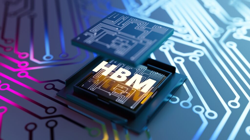
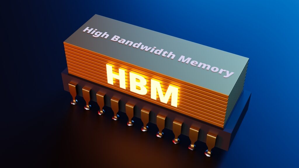
HBM is a memory technology that stacks multiple DRAM chips vertically and connects them with a very wide data bus.
Main features:
・3D stacking of memory chips
・Vertical wiring using TSVs
・A wide memory bus
This makes it possible to achieve far higher bandwidth than conventional memory.
【2】Differences from Conventional Memory
Conventional memory (such as DDR) is mainly placed on the board and connected to the chip with relatively long wiring.
HBM, on the other hand, is placed close to the GPU or AI chip and connected directly on an interposer.
Main differences:
・Short wiring distance
・Wide data bus
・High power efficiency
This structure allows HBM to achieve extremely high memory bandwidth.
【3】HBM Generations
HBM performance has improved with each generation.
Representative generations:
・HBM (first generation)
・HBM2
・HBM2E
・HBM3
・HBM3E
In the latest generations, some achieve bandwidth on the order of 1TB/s with a single memory stack.
【4】AI Chips and HBM
AI training requires processing large amounts of data at high speed.
For this reason, many AI accelerators have adopted HBM.
Representative examples:
・NVIDIA AI GPUs
・AMD AI accelerators
・Various AI server chips
In AI servers, configurations in which multiple HBM stacks are placed around the GPU have become common.
【5】Design Challenges Brought by HBM
The adoption of HBM has also created new challenges for semiconductor design.
Main challenges:
・The need for advanced packaging technology
・Greater difficulty of thermal design
・High-density wiring design
・Higher costs
In particular, HBM is often used in combination with 2.5D packaging, further increasing the importance of packaging technology.
The evolution of AI semiconductors is supported not only by transistor performance but also by integration technology for memory and packaging.
【6】Summary
・Memory bandwidth is important in AI computation
・HBM is a 3D-stacked memory technology
・HBM is widely adopted in AI chips
・Combination with advanced packaging is indispensable
Comprehension Check
1.Why is memory bandwidth important in AI computation?
2.What are the structural differences between HBM and conventional memory?
3.Why is HBM combined with advanced packaging technology?
Column Supervisor: Koji Kakumoto (President, OTIS Co., Ltd.)
After studying abroad and working in planning and development at a trading company, he joined OTIS Co., Ltd. in 2011. While primarily working in the Corporate Planning Department, he has also served concurrently in manufacturing and technical divisions, and since 2018 has served as President, working to drive business growth and strengthen the organization.
This article is a general technical explanation intended for educational purposes and does not refer to any specific company, product, or technology.