【1】Why Advanced Packaging Has Become Important
In semiconductors for AI and data centers, the following requirements are rising rapidly.
Main requirements:
・High memory bandwidth
・High-speed chip-to-chip communication
・Handling high heat generation
・Miniaturization
To achieve these, not only the performance of a single chip but also packaging technology that efficiently connects multiple chips is indispensable.
【2】2.5D Packaging
In 2.5D packaging, multiple chips are placed on a substrate called a silicon interposer.
Structural features:
・Chips are placed side by side
・Connected with silicon wiring
・High-density wiring is possible
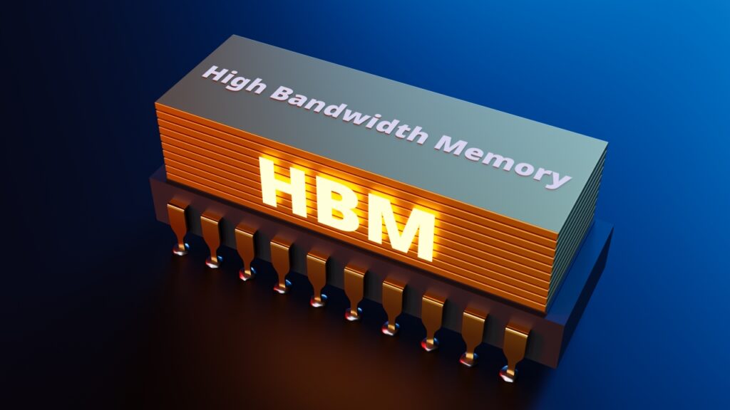
This method is widely used, for example, to connect GPUs and HBM memory.
Representative examples:
・TSMC CoWoS
・Samsung I-Cube
In AI chips, 2.5D packaging has become an important technology for connecting HBM memory at high speed.
【3】3D Packaging
In 3D packaging, higher integration is achieved by stacking chips vertically.
Main technologies:
・TSV (Through Silicon Via)
・Hybrid bonding
・Die stacking
This makes it possible to shorten the distance between chips drastically, improving communication speed and power efficiency.
Representative examples:
・Intel Foveros
・TSMC SoIC
【4】Fan-Out Packaging
Fan-out is a packaging technology that increases wiring density using a redistribution layer (RDL).
Features:
・No interposer required
・Can be made thinner
・High-density wiring
It is widely adopted in processors for smartphones and other devices.
Representative examples:
・TSMC InFO
・Samsung eWLB
【5】An Era in Which Advanced Packaging Determines Semiconductor Performance
In AI chips, there are more and more cases in which the package structure as a whole, rather than the chip alone, determines performance.
Particularly important factors:
・Chip-to-chip communication speed
・Memory bandwidth
・Thermal design
・Power delivery
In other words, we are now in an era in which semiconductor performance is determined not only by transistor design but by the combined strength of packaging, materials, and assembly technology.
This trend also has important implications for materials manufacturers and companies with processing technologies.
【6】Summary
・Advanced packaging is an important technology that determines semiconductor performance
・2.5D and 3D packaging are widely adopted in AI chips
・2.5D technology is important for HBM connections
・It is an era in which package design determines system performance
Comprehension Check
1.Why is advanced packaging important for AI chips?
2.What is the difference between 2.5D packaging and 3D packaging?
3.Why is packaging technology becoming important for semiconductor performance?
Column Supervisor: Koji Kakumoto (President, OTIS Co., Ltd.)
After studying abroad and working in planning and development at a trading company, he joined OTIS Co., Ltd. in 2011. While primarily working in the Corporate Planning Department, he has also served concurrently in manufacturing and technical divisions, and since 2018 has served as President, working to drive business growth and strengthen the organization.
This article is a general technical explanation intended for educational purposes and does not refer to any specific company, product, or technology.