【1】Why HBM / Chiplets Became Necessary
① Memory bandwidth became the bottleneck
In AI chips:
・Computing performance (FLOPS) has improved exponentially
・Memory bandwidth is relatively hard to increase
As a result, a state arises in which computation is possible but the data does not arrive.
→ It became necessary to place memory close to the CPU/GPU.
② The limits of the monolithic SoC
With single-chip integration (monolithic), the following are unavoidable:
・Ballooning chip size
・Worsening yield
・Soaring costs
→ This led to the idea of dividing by function and connecting them in back-end processes.
【2】What Is HBM (High Bandwidth Memory)?
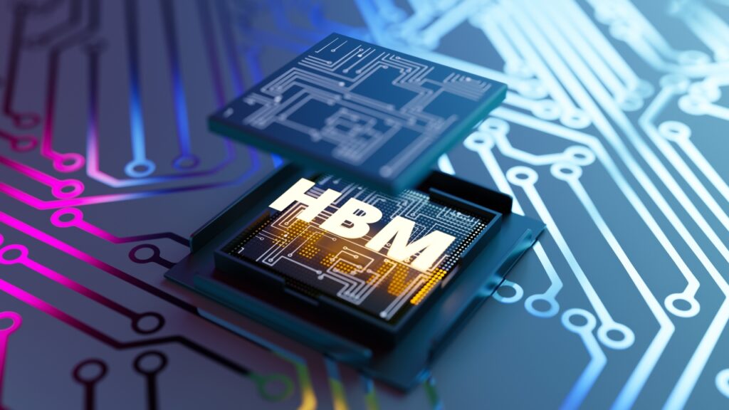
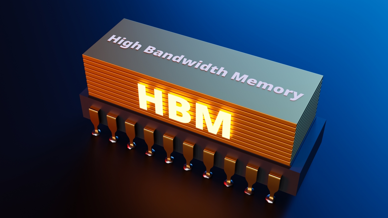
HBM is ultra-high-speed memory in which DRAM is stacked vertically and connected with TSVs.
Features:
・Extremely wide I/O width (thousands of bits)
・Low clock speed and low power consumption
・Placed close to the GPU / AI accelerator
As a result:
・Bandwidth: on the order of several TB/s
・Power efficiency: greatly improved compared with conventional DDR
It is effectively an essential component in AI chips.
【3】The Concept of Chiplet Architecture
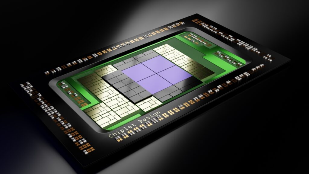
A chiplet is a design philosophy in which small dies (chips) divided by function are connected with high-density packaging to operate as a single system.
Examples of division:
・Compute die
・I/O die
・Memory die
・Accelerator die
Advantages of Chiplets
・Higher yield (smaller dies)
・Process optimization (leading-edge for compute, mature for I/O)
・Design reusability
・Shorter development periods
Challenges of Chiplets
・Interconnect delay
・Power consumption
・Packaging difficulty
・More complex testing
→ Packaging technology determines performance.
【4】2.5D Packaging (Interposer Technology)
2.5D is a structure in which multiple chips are placed side by side and connected on a silicon interposer.
Representative examples:
・CoWoS (TSMC)
・EMIB (Intel)
・I-Cube (Samsung)
Features:
・Ultra-fine wiring
・High speed and low latency
・Highly compatible with HBM
The mainstream structure for AI chips.
【5】3D Packaging (TSV Stacking)
3D is a method in which chips are stacked vertically and connected directly with TSVs.
Features:
・Shortest wiring
・Highest bandwidth
・Lowest latency
On the other hand:
・Heat dissipation is extremely difficult
・Reliability evaluation is demanding
・High yield risk
→ Often limited to specific applications or still at the research stage.
【6】The Biggest Challenges in the Era of HBM / Chiplets
(1) Yield and Cost
・Multiple dies are integrated into one package
・If any one is defective → the entire package is defective
Known Good Die (KGD) is essential.
(2) Thermal Design
・High heat density from HBM + compute dies
・Local hot spots occur
→ Heat dissipation structures and placement design determine performance.
(3) Increasingly Complex SI / PI / EMI
・Faster chip-to-chip interfaces
・Increased supply current
→ Package co-design is a prerequisite.
【7】Latest Trends
・Evolution to HBM3 / HBM3E / HBM4
・Larger interposers
・Research on organic interposers
・Chiplet standardization (UCIe)
・Integration with optical I/O (in the future)
【8】Summary
・In the AI era, “connection” matters more than “computation”
・HBM is the key to eliminating the bandwidth bottleneck
・Chiplets are a realistic solution for cost and yield
・2.5D is mainstream; 3D is highly difficult
・Packaging technology determines system performance
Comprehension Check
1.Why has HBM become essential for AI chips?
2.Why does the chiplet approach lead to improved yield?
3.What is the biggest difference between 2.5D and 3D packaging?
Column Supervisor: Koji Kakumoto (President, OTIS Co., Ltd.)
After studying abroad and working in planning and development at a trading company, he joined OTIS Co., Ltd. in 2011. While primarily working in the Corporate Planning Department, he has also served concurrently in manufacturing and technical divisions, and since 2018 has served as President, working to drive business growth and strengthen the organization.
This article is a general technical explanation intended for educational purposes and does not refer to any specific company, product, or technology.