【1】What Is the Chiplet Approach?
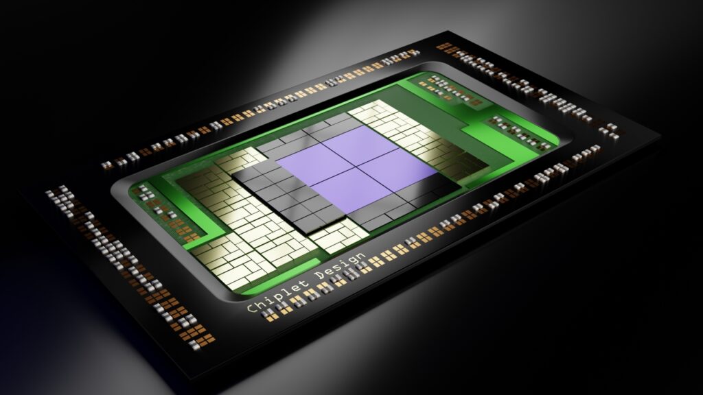
Conventional semiconductors have been built as a single large chip (monolithic). However, due to the limits of scaling, rising costs, and worsening yields,
a new philosophy emerged: rather than making one large chip, it is more efficient to divide it into smaller pieces and connect them.
This is the chiplet approach.
The chiplet approach offers major advantages:
● Chips from different process nodes can be combined
● Leading-edge processes are used only where they are needed
● Yield improves and costs can be optimized
● The scalability of AI/GPU/CPU products increases dramatically
Representative examples: AMD (Ryzen), Intel (Meteor Lake), NVIDIA (Grace Hopper), Apple (M series)
【2】Fundamentals of 2.5D Packaging (The Interposer Approach)
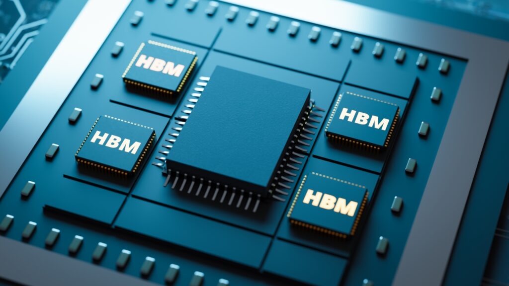
In 2.5D packaging, chips are placed side by side and connected at high speed on a silicon substrate (interposer).
Features:
● A silicon interposer with TSVs serves as the wiring
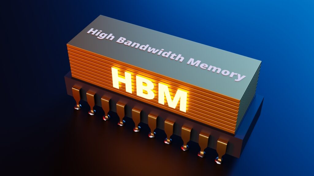
● Extremely wide-bandwidth communication is possible (the foundational technology for HBM)
● The distance between chiplets is short (low latency)
Applications:
● HBM + GPU (NVIDIA, AMD)
● CPUs for HPC
● Large-scale AI accelerators
2.5D has become the “standard structure” of today’s AI semiconductors.
【3】Features of 3D Packaging (Stacked Connections)
3D packaging stacks chips vertically, enabling higher-density, higher-bandwidth connections.
Representative examples:
● DRAM stacked directly on logic (hybrid bonding)
● Memory such as SRAM integrated on top of logic
● Next-generation HPC and AI processors
3D stacking goes beyond conventional package structures, delivering:
● Ultra-low latency
● Ultra-wide bandwidth
● Dramatically shorter wiring lengths
● Smaller size
However, heat has become the biggest challenge.
【4】Chiplet Interconnect Technologies (UCIe and Hybrid Bonding)
(1) UCIe (Universal Chiplet Interconnect Express)
A standard interface specification for chiplets that semiconductor companies can use in common.
Objectives:
・Combining chips from different manufacturers
・Expanding the supply chain
・Reducing development costs
In the future, it is said that a world will emerge in which companies can freely combine “a CPU from Company A, an AI chip from Company B, and I/O from Company C.”
(2) Hybrid Bonding
The 3D interconnect technology currently attracting the most attention.
Features:
・Cu and the insulating film are “bonded directly”
・Connections can be made over extremely short distances, greatly reducing resistance and parasitic capacitance
・Enables even higher-density integration than TSV
TSMC, Intel, and Samsung are accelerating investment toward volume production.
【5】The Changes Brought by Chiplets / 2.5D / 3D
(1) A Major Transformation in Architecture
“From the monolithic era → to the chiplet era”
This change will transform even the structure of the semiconductor industry itself.
(2) A Leap in Design Freedom
・Leading-edge nodes only for the parts that need them
・Mature nodes are fine for analog
・Memory placed close by for higher speed
Rationality and performance can be achieved at the same time.
(3) Manufacturing Becomes More Specialized
Within the same package:
・Leading-edge logic: TSMC
・Memory: Samsung / SK hynix
・I/O: GlobalFoundries
— a global division of labor like this becomes possible.
(4) An Essential Technology for the AI Era
The AI servers that run ChatGPT are premised on the combination of HBM × GPU × 2.5D / 3D.
The more AI demand grows, the more the chiplet approach becomes an unavoidable core technology.
【6】Challenges and Constraints
While the benefits are significant, the following challenges exist:
● Heat (more severe in the vertical direction)
● Complex design rules
● The yield of the entire chiplet assembly is affected
● The difficulty of the packaging process rises sharply
● Stress caused by material properties (CTE differences / thermal expansion)
Heat in particular is a serious problem, and the industry is now seeking chiplets that can be cooled.
【7】Summary
● Chiplets are a design philosophy for overcoming the limits of huge chips
● 2.5D is the interposer approach supporting the HBM era
● 3D offers ultra-high density, but heat and yield are challenges
● UCIe and hybrid bonding are the next-generation interconnect technologies
● The main battleground for semiconductors in the AI era is “Chiplet × 2.5D × 3D”
Comprehension Check
1.What is the main background behind the emergence of the chiplet approach?
2.Explain why an interposer is used in 2.5D packaging.
3.Name one feature of hybrid bonding.
Column Supervisor: Koji Kakumoto (President, OTIS Co., Ltd.)
After studying abroad and working in planning and development at a trading company, he joined OTIS Co., Ltd. in 2011. While primarily working in the Corporate Planning Department, he has also served concurrently in manufacturing and technical divisions, and since 2018 has served as President, working to drive business growth and strengthen the organization.
This article is a general technical explanation intended for educational purposes and does not refer to any specific company, product, or technology.