【1】What Is Semiconductor Manufacturing Equipment?
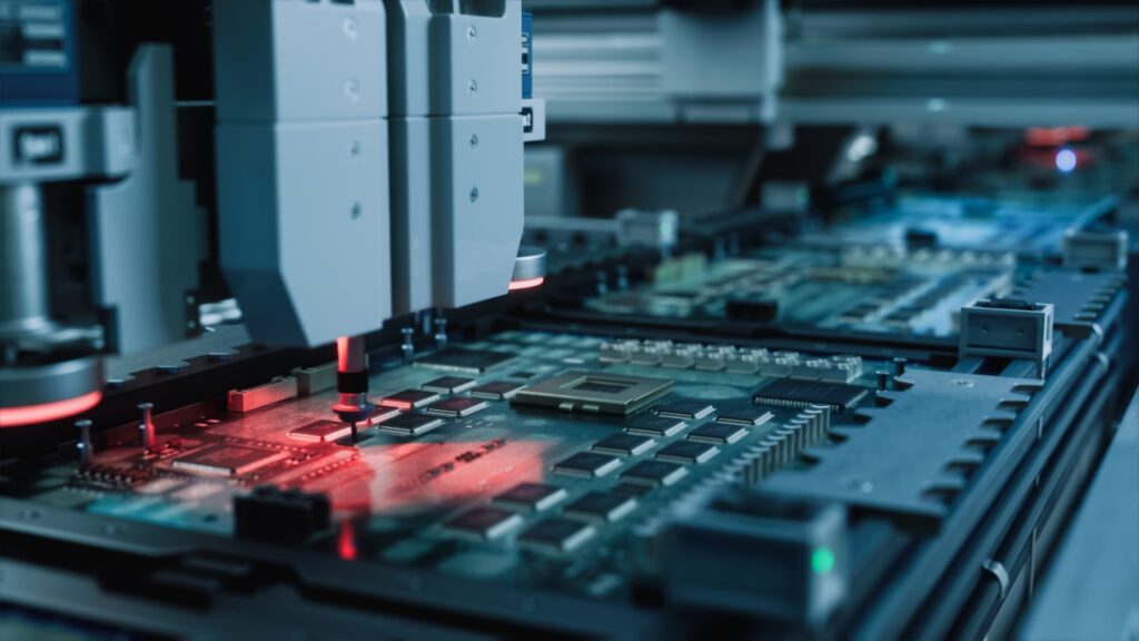
Semiconductor manufacturing requires hundreds of process steps.
The equipment used in each of these steps is semiconductor manufacturing equipment.
Typical processes:
・Lithography
・Deposition
・Etching
・Ion implantation
・CMP
・Cleaning
・Inspection
A single factory has hundreds to thousands of tools lined up.
【2】Lithography Equipment
Equipment that transfers circuit patterns onto the wafer.
It is the core technology of scaling.
Representative company:
・ASML (Netherlands)
An EUV lithography tool costs 30 billion yen or more per unit.
ASML is the only company in the world that can manufacture it.
【3】Deposition Equipment
The process of forming thin films.
Applications:
・Insulating films
・Wiring materials
・Gate materials
Main methods:
・CVD
・PVD
・ALD
Representative companies:
・Applied Materials
・Tokyo Electron
【4】Etching Equipment
The process of removing unnecessary parts.
Roles:
・Circuit formation
・Trench processing
・Via formation
Microfabrication requires atomic-level control.
Representative companies:
・Lam Research
・Tokyo Electron
【5】Ion Implantation Equipment
The process that creates semiconductor characteristics.
Roles:
・Doping
・Adjusting electrical characteristics
Trace elements are implanted into silicon as high-speed ions.
Representative companies:
・Applied Materials
・Axcelis
【6】CMP Equipment
CMP stands for Chemical Mechanical Polishing.
It planarizes the wafer surface at the nanometer level.
This process is indispensable for multilayer wiring.
Representative companies:
・Applied Materials
・EBARA
【7】Cleaning Equipment
In semiconductor manufacturing, fine particles and contamination must be completely removed.
Roles:
・Particle removal
・Chemical cleaning
・Drying
Representative companies:
・SCREEN
・Tokyo Electron
This is an area where Japanese companies are strong.
【8】Inspection Equipment
Equipment that detects tiny defects.
Inspection targets:
・Particles
・Pattern defects
・Wiring breaks
Detecting nano-scale defects requires extremely advanced optical technology.
Representative companies:
・KLA
・Hitachi High-Tech
【9】Characteristics of the Equipment Industry
Characteristics of the semiconductor equipment industry:
・Ultra-high technology
・Low volume, high price
・Oligopolistic market
A single tool often costs several billion yen or more.
【10】Why Equipment Manufacturers Are Important
The reason is clear.
Equipment performance determines the limits of semiconductors.
Examples:
・EUV lithography → limits of scaling
・Etching → high-aspect-ratio processing
・Deposition → atomic-layer control
In other words, equipment creates technological progress.
【11】Strengths of Japanese Companies
Japan is also strong in the equipment field.
Representative companies:
・Tokyo Electron
・SCREEN
・Hitachi High-Tech
・EBARA
・Canon
They have particularly high global shares in
・Cleaning equipment
・Deposition equipment
・Metrology equipment.
【12】Summary
・Semiconductor manufacturing equipment is the core of processing
・Many types of equipment are needed, such as lithography, deposition, and etching
・Equipment performance determines technological limits
・The equipment industry is an oligopolistic market
・Japanese companies are also strong worldwide
Comprehension Check
1.What is the role of semiconductor manufacturing equipment?
2.Why is EUV lithography equipment important?
3.Why does equipment performance determine the limits of semiconductor technology?
Column Supervisor: Koji Kakumoto (President, OTIS Co., Ltd.)
After studying abroad and working in planning and development at a trading company, he joined OTIS Co., Ltd. in 2011. While primarily working in the Corporate Planning Department, he has also served concurrently in manufacturing and technical divisions, and since 2018 has served as President, working to drive business growth and strengthen the organization.
This article is a general technical explanation intended for educational purposes and does not refer to any specific company, product, or technology.