【1】What Are Semiconductor Materials?
The materials used in semiconductor manufacturing can be broadly classified as follows.
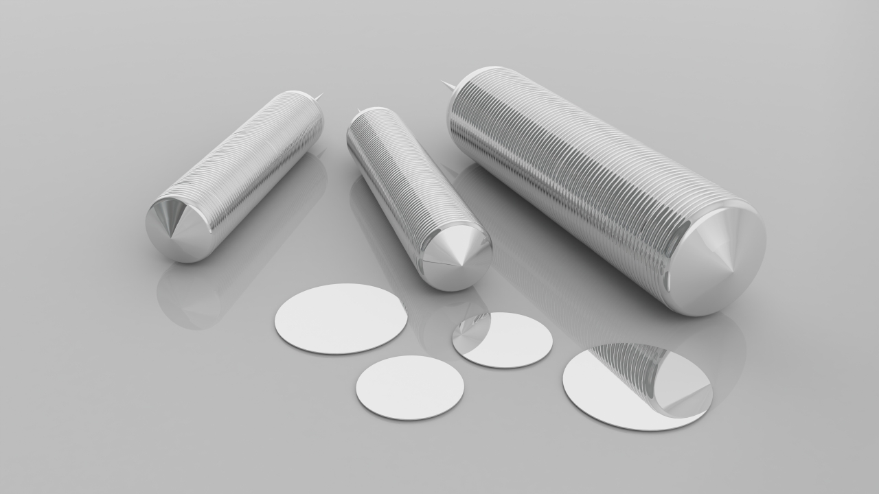
・Wafer materials
・Photoresists
・Process gases
・CMP materials
・Encapsulation materials
・Package materials
These are combined to create structures with nanometer precision.
【2】Silicon Wafers
The material that serves as the substrate of a semiconductor.
Features:
・High-purity single crystal
・300mm diameter is mainstream
・Nanometer-level flatness
Representative companies:
・Shin-Etsu Chemical
・SUMCO
These two companies account for the majority of the global market share.
【3】Photoresists
A photosensitive material used in the lithography process.
Roles:
・Forming circuit patterns
・Determining the precision of microfabrication
In the EUV generation, resist performance determines how far scaling can go.
Representative companies:
・JSR
・Tokyo Ohka Kogyo
・Shin-Etsu Chemical
【4】Process Gases
Many specialty gases are used in semiconductor manufacturing.
Examples:
・Silane
・Ammonia
・Fluorine-based gases
・Argon
Applications:
・Deposition
・Etching
・Cleaning
Ultra-high purity is required.
【5】CMP Materials
CMP stands for Chemical Mechanical Polishing.
It is the process of planarizing the wafer surface at the atomic level.
Required materials:
・Slurry
・Pads
Flatness determines wiring precision.
【6】Cleaning Chemicals
In semiconductor manufacturing, fine particles and metal contamination must be completely removed.
Main chemicals:
・Sulfuric acid
・Hydrogen peroxide
・Hydrofluoric acid
・Ammonia
Even trace impurities affect yield.
【7】Encapsulation Materials (Mold)
Materials that protect the chip in the back-end process.
Roles:
・Mechanical protection
・Protection against humidity
・Heat dispersion
Epoxy resin is mainly used.
【8】Package Materials
Materials used in the packaging process.
Examples:
・Underfill
・TIM (thermal interface material)
・Solder materials
・Substrate materials
In AI chips, the importance of thermally conductive materials is increasing sharply.
【9】Why Japanese Companies Are Strong
There are three reasons.
・High-purity chemical technology
・Accumulated materials research
・Quality control capability
In materials, many years of know-how is the source of competitiveness.
New entry is difficult.
【10】The Importance of Material Supply
In the semiconductor supply chain, when materials stop, factories stop.
Examples:
・Resist supply
・Wafer shortages
・Gas supply
For this reason, materials companies are the foundational infrastructure of the industry.
【11】The Future of Materials Technology
Materials that will become important in the future:
・High-k materials
・Low-k materials
・SiC wafers
・GaN substrates
・Thermally conductive materials
Materials for power semiconductors in particular are growing rapidly.
【12】Summary
・Semiconductors are a huge materials industry
・They are composed of many kinds of materials, such as wafers, resists, and gases
・Material quality determines yield
・Japanese companies are strong in the materials field
・Next-generation materials are the future axis of competition
Comprehension Check
1.Why are semiconductor materials important?
2.What is the role of photoresist?
3.Why are Japanese companies strong in the materials field?
Column Supervisor: Koji Kakumoto (President, OTIS Co., Ltd.)
After studying abroad and working in planning and development at a trading company, he joined OTIS Co., Ltd. in 2011. While primarily working in the Corporate Planning Department, he has also served concurrently in manufacturing and technical divisions, and since 2018 has served as President, working to drive business growth and strengthen the organization.
This article is a general technical explanation intended for educational purposes and does not refer to any specific company, product, or technology.