【1】What Is an OSAT?
An OSAT is a company that specializes in the back-end process of semiconductors.
Main roles:
・Packaging (Assembly)
・Electrical testing (Test)
・Reliability evaluation
OSATs receive wafers from fabless companies and IDMs and finish them into final semiconductor components.
【2】The Basic Flow of the Back-End Process
The typical flow of the back-end process:
・Wafer test (Wafer Probe)
・Dicing (cutting the chips)
・Die attach
・Wire bonding / bump connection
・Encapsulation (molding)
・Final test
Defective chips are removed here.
【3】Representative OSAT Companies
The world’s major OSAT companies:
・ASE Technology (Taiwan)
・Amkor (USA / South Korea)
・JCET (China)
・SPIL (Taiwan)
ASE in particular is the world’s largest OSAT company.
【4】Why OSATs Exist
There are three main reasons.
・Back-end equipment is expensive
・Packaging technology is becoming more advanced
・The advantages of volume production scale
Because foundries concentrate on the front-end process, a structure in which the back-end process is outsourced has been established.
【5】The Role of Packaging
Packaging has four roles.
・Protecting the chip
・Electrical connection
・Heat dissipation
・Ensuring mechanical strength
In other words, it is the process that puts semiconductors into a usable form.
【6】The Evolution of Packaging Technology
Conventional packages:
・Wire bonding
・QFN
・BGA
Advanced packages:
・Fan-out
・2.5D
・3D stacking
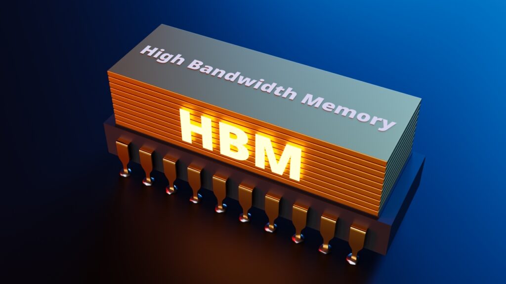
・HBM
Packaging technology is becoming the key to improving performance.
【7】The AI Era and OSATs
In AI chips,
・Huge chips
・Ultra-high currents
・High heat density
become problems.
For this reason, back-end technologies such as
・HBM stacking
・2.5D packaging
・Large interposers
determine performance.
【8】The Relationship Between OSATs and Foundries
Traditionally, the division of labor was:
・Foundry → Wafer manufacturing
・OSAT → Packaging
Recently, however, foundries have entered packaging.
Examples:
・TSMC CoWoS
・Intel Foveros
The competitive structure is changing.
【9】The OSAT Business Model
The OSAT profit structure:
・High-volume processing
・Low cost
・High yield
Profit margins are lower than those of foundries.
Therefore, production efficiency is important.
【10】Technical Challenges for OSATs
Main challenges:
・Thermal management
・Power supply noise
・Signal delay
・High-density wiring
For AI chips, thermal design is the biggest challenge.
【11】The Future of OSATs
Future directions:
・3D packaging
・Chiplet interconnection
・Optical I/O packaging
・Liquid-cooled packaging
Packaging is said to be the last performance bottleneck.
【12】Summary
・OSATs are companies specializing in the semiconductor back-end process
・They are responsible for packaging and testing
・It is the process that turns chips into products
・In the AI era, packaging determines performance
・Competition with foundries is intensifying
Comprehension Check
1.What are the main roles of an OSAT company?
2.Why does packaging become important for AI chips?
3.How is the relationship between foundries and OSATs changing?
Column Supervisor: Koji Kakumoto (President, OTIS Co., Ltd.)
After studying abroad and working in planning and development at a trading company, he joined OTIS Co., Ltd. in 2011. While primarily working in the Corporate Planning Department, he has also served concurrently in manufacturing and technical divisions, and since 2018 has served as President, working to drive business growth and strengthen the organization.
This article is a general technical explanation intended for educational purposes and does not refer to any specific company, product, or technology.