【1】What Is a Package Substrate?
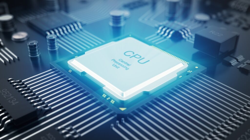
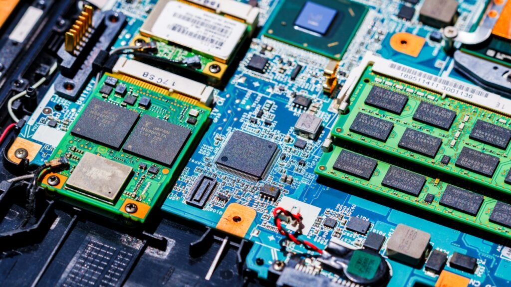
A package substrate is an intermediate substrate that connects a semiconductor chip to a printed circuit board.
Roles:
・Signal wiring
・Power delivery
・Securing the chip
・Heat dispersion
Inside electronic equipment, it bridges the chip and the motherboard.
【2】The Basics of Package Structure
Semiconductor products have a three-layer structure of
・Chip
・Package substrate
・Printed circuit board
Flow:
Chip → Package substrate → System board
This structure is the foundation of electronic equipment.
【3】ABF Substrates
Substrates used for high-performance chips.
ABF stands for Ajinomoto Build-up Film, an insulating material.
Features:
・Fine wiring
・High-layer-count structure
・High reliability
It is the standard substrate for high-performance processors such as CPUs and GPUs.
【4】High-Layer-Count Substrates
Leading-edge chips have an enormous number of wires.
For this reason, multilayer substrates with
・10 layers
・20 layers
・30 or more layers
are used.
The more layers there are, the better the
・Signal wiring
・Power stability
become.
【5】Fine Wiring Technology
Scaling is also progressing in package substrates.
Typical indicators:
・Line width
・Space
In recent years, wiring of 10µm or less has also come into use.
This is for high-density chip connections.
【6】RDL (Redistribution Layer)
RDL stands for Redistribution Layer.
It is a layer that relocates the chip’s connection points to external wiring.
Roles:
・Expanding chip connections
・Fan-out packages
・High-density connections
It is an important technology in advanced packaging.
【7】AI Chips and the Importance of Substrates
In AI chips,
・High currents
・High signal speeds
・Huge chips
become problems.
For this reason, substrates are required to provide
・Low noise
・Low latency
・High-current capability.
【8】HBM and Interposers
AI chips use HBM (High Bandwidth Memory).
With HBM,
・The GPU
・The memory
are connected with a silicon interposer.
This is 2.5D packaging technology.
【9】Major Package Substrate Manufacturers
Representative companies:
・Ibiden (Japan)
・Shinko (Japan)
・Unimicron (Taiwan)
・Nan Ya PCB (Taiwan)
Japanese companies are strong in high-performance substrates.
【10】The Supply Constraint Problem
Package substrates have fallen into short supply due to the AI boom.
Causes:
・Demand for HBM
・Demand for GPUs
・Shortage of manufacturing equipment
For this reason, substrates can become a bottleneck in semiconductor supply.
【11】Future Substrate Technologies
Next-generation technologies:
・Glass substrates
・High-frequency substrates
・Optical interposers
・Liquid-cooled packages
We are entering an era in which semiconductor performance is determined by packages and substrates.
【12】Summary
・Package substrates bridge the chip and the system
・ABF substrates are the standard for high-performance chips
・Fine wiring and higher layer counts are advancing
・Substrate performance is important for AI chips
・Japanese companies are strong in high-performance substrates
Comprehension Check
1.What is the role of a package substrate?
2.Why are ABF substrates used?
3.Why does substrate technology become important for AI chips?
Column Supervisor: Koji Kakumoto (President, OTIS Co., Ltd.)
After studying abroad and working in planning and development at a trading company, he joined OTIS Co., Ltd. in 2011. While primarily working in the Corporate Planning Department, he has also served concurrently in manufacturing and technical divisions, and since 2018 has served as President, working to drive business growth and strengthen the organization.
This article is a general technical explanation intended for educational purposes and does not refer to any specific company, product, or technology.