■ What Is Microfabrication?
The term microfabrication has a very broad meaning.
Nano-processing of semiconductors is sometimes called microfabrication.
It can also refer to precision machining of metal parts.
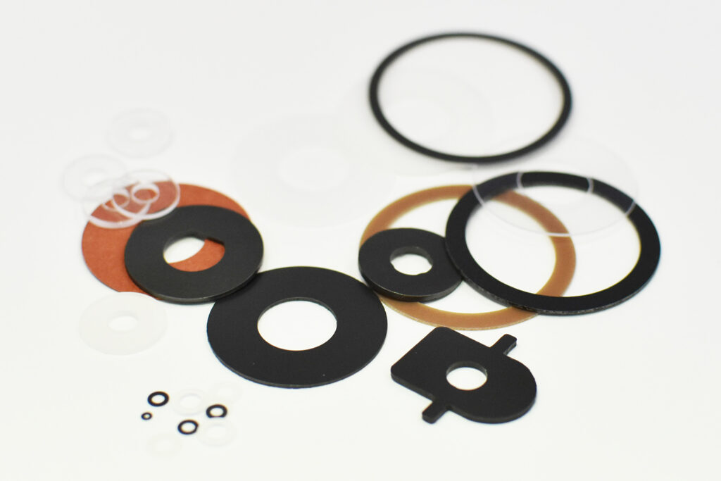
In the area OTIS handles, the focus is on processing thin materials such as
films,
adhesives,
metal foils,
TIM,
graphite,
and foams
with high precision into
tiny holes,
narrow widths,
complex outer shapes,
and narrow spacing.
In other words, OTIS’s microfabrication can be thought of as the technology of processing thin-film functional materials into the required micro shapes.
■ Why Is Microfabrication Needed in Thermal Management?
Thermal management tends to bring to mind large heat sinks and cooling plates.
But in reality, small functional components are needed
right next to heat sources,
in gaps between components,
around sensors,
and around electrodes.
For example,
placing TIM on only part of an IC,
opening only at the sensor position,
leaving film only where insulation is needed,
and extending graphite only in the direction heat should be released.
Such designs require fine shape processing.
In other words, the advancement of thermal management progresses not only through larger cooling devices, but also through miniaturization of components around heat sources.
■ The Smaller the Heat Source, the Higher the Heat Density Tends to Be
Even with the same 10 W of heat generation,
10 W from a 100 mm square
and 10 W from a 10 mm square
mean different things.
The more heat is concentrated in a small area, the greater the local heat flux.
Then slight differences in
TIM position,
contact area,
and heat spreader shape
become more influential.
In other words, the smaller the heat source, the more directly fine processing accuracy connects to thermal performance.
■ In Small Components, 0.1 mm Means More
A 100 mm component shifts by 0.1 mm.
The impact may be relatively small.
But a 2 mm-wide component shifts by 0.1 mm.
That is 5% of the width.
In other words, even with the same processing error, the smaller the component, the larger the relative error.
Around semiconductors and sensors, dimensions such as
0.1 mm
and 0.05 mm
can become the functional area itself.
That is why in microfabrication, rather than simple dimensional tolerances,
it is necessary to be aware even of the error rate relative to product size.
■ Narrow TIM Shapes Are Sometimes Needed
Around heat-generating components, there are
connectors,
chip components,
wiring,
sensors, and so on.
When TIM is to be placed only between them,
narrow shapes a few mm wide may be needed.
But TIM is soft.
Making it narrow increases problems such as
stretching,
deforming,
being hard to peel,
and being hard to transport.
In other words, being able to cut it narrow is not enough. It must be possible to handle it while it remains narrow.
■ With Graphite, Narrow Heat Paths Are Sometimes Created
Graphite is extended from the heat source to the enclosure.
But there are other components along the way.
So narrow paths,
curved paths,
and notches are created.
This is like creating wiring for heat.
Just as electrical circuits have wiring patterns,
paths are created for heat to flow in the required direction.
In other words, microfabrication can also be the technology of designing the path for heat as a shape.
■ Making It Too Narrow Also Makes Heat Flow Harder
Miniaturization increases placement freedom.
But the cross-sectional area through which heat flows becomes smaller.
For example, if graphite is made very narrow,
it can pass through narrow spaces.
On the other hand, that narrow part may become a bottleneck in the heat path.
In other words, we want to make it narrow.
But we want a lot of heat to flow. There is this contradiction.
In microfabrication, it is necessary to consider not the smallest shape that can be processed, but the smallest shape that can maintain function.
■ Fine Slits Also Have Roles
Slits are made in films and adhesives.
Then they can be given functions such as
releasing air,
making bending easier,
relieving stress,
and allowing partial deformation.
In other words, slits are not just cuts.
For example, when applying a large-area sheet to a curved surface, partial slits can sometimes increase conformability.
Microfabrication can create movements and functions that the material itself does not have.
■ Opening Processing Also Has Functions
Small openings are made in an insulating film.
Only that part contacts the electrode.
Only the thermally conductive material is exposed.
Only the sensor is exposed.
In such structures, the opening position becomes very important.
If it shifts slightly, a necessary place is insulated.
Conversely, a place that should be insulated is exposed.
In other words, fine opening processing can be thought of as processing that spatially separates functions ON and OFF.
■ In Insulation, Microfabrication Accuracy Connects to Safety
Around high-voltage components, insulation distance is important.
If the insulating film’s
outer shape,
openings,
and hole positions
shift, the required insulation distance may not be secured.
Furthermore, with miniaturization, the insulation distance itself becomes smaller.
That is why
a 0.2 mm positional deviation
and a 0.1 mm burr
take on relatively greater meaning.
In other words, microfabrication relates not only to thermal performance but also to electrical safety performance.
■ The More Miniaturized, the Less Burrs Can Be Ignored
For example, a 10 mm-wide component has a 0.02 mm burr.
The impact may be limited.
But if a 0.2 mm-wide narrow part has a 0.02 mm burr, that is 10% of the width.
Furthermore, with metal foil, that burr may damage the insulating film.
In other words, with miniaturization,
small processing defects become relatively larger.
That is why in microfabrication, edge quality matters, not just dimensions.
■ Tiny Holes Also Make Slug Control After Processing Difficult
Holes a few mm in diameter,
or smaller, are processed.
Then the slugs also become small.
Those slugs may
stick to the adhesive surface,
remain on the film,
or transfer to other products.
Especially with adhesives, small slugs stick and are hard to remove.
In other words, in microfabrication,
both being able to process it and being able to completely remove unwanted matter are important.
■ The Smaller the Hole, the Harder It Is on the Die Side Too
When punching small-diameter holes, the punch on the die side also becomes thin.
As it becomes thinner, risks increase such as
lower rigidity,
wear,
breaking,
and positional deviation.
In other words, the smaller the product shape, the greater the impact on die design and die life.
Microfabrication is also the technology of balancing product miniaturization and die durability.
■ The "Minimum Processable Dimension" and the "Minimum Mass-Producible Dimension" Differ
A single prototype can be processed.
But processing tens of thousands in volume production brings problems of
die wear,
material variation,
waste stripping,
and transport.
That is why the information
“processable down to a minimum of 0.1 mm”
alone is not enough.
What matters to the customer is
the dimensions at which the required quantity can be made stably at the required quality.
■ Microfabrication Limits Differ by Material
PET.
PI.
Copper foil.
Aluminum foil.
Adhesive.
Foam.
TIM.
Graphite.
Each differs in
hardness,
brittleness,
elongation,
thickness,
and tackiness.
Even with the same 0.5 mm width,
it can be processed stably with one material
and be difficult with another.
This happens.
In other words, it is difficult to express microfabrication capability with a single number.
It must be considered as material × thickness × shape × quantity.
■ Microfabrication of Soft Materials Is Difficult
Soft TIM is die-cut narrow.
The material escapes sideways before the blade enters.
It is compressed.
It springs back after cutting.
As a result,
dimensions are not stable.
Edges deform.
This happens.
In other words, with soft materials,
more than blade accuracy,
how to hold the material and cut it without deforming it is important.
■ Brittle Materials Have a Different Difficulty
With graphite and similar materials,
when made narrow, they
chip easily,
crack easily,
and break easily during transport.
In other words, soft materials and brittle materials have difficulties in opposite directions.
In microfabrication, it is necessary to understand material properties and change conditions.
■ With Thin Metal Foil, "Cutting" and "Deformation" Occur Simultaneously
When copper foil or aluminum foil is processed into fine shapes,
the foil itself can deform from the cutting force.
In narrow parts, it may
twist,
wave,
and warp.
Even if the dimensions are correct, poor flatness makes it hard to apply in later processes.
In other words, in fine metal foil processing,
not only two-dimensional dimensions but three-dimensional deformation also becomes quality.
■ With Miniaturization, Adhesive "Squeeze-Out" Also Stands Out
0.1 mm of adhesive squeezes out from a 1 mm-wide adhesive component.
That is large in area ratio.
Furthermore, it may
stick to surrounding components,
affect insulation distance,
and stick to equipment.
In other words, in fine adhesive components, not only the outer shape but the positional accuracy of the adhesive itself is important.
■ Partial Adhesion and Microfabrication Go Well Together
When adhesive does not need to be placed over the entire surface,
only the necessary parts can be made adhesive.
For example,
adhesive only on the outer 1 mm,
non-adhesive in the center.
That is the structure.
This may enable
lower thermal resistance,
fewer air bubbles,
and improved peelability.
In other words, microfabrication can also be the technology of placing adhesive functions only where needed.
■ Placing Heat, Insulation and Adhesion Finely
For example, within a single small component, a structure is made with
center = thermal conduction,
perimeter = insulation,
part = adhesion.
This is hard to achieve with a single material.
Multiple materials must be placed and laminated with high precision.
In other words, as microfabrication advances, the value of processing shifts from simple outer shape processing to
placement of functions in micro areas.
■ Microfabrication Is Important Around Sensors
Temperature sensors.
Pressure sensors.
Optical sensors.
Biosensors.
Around these, multiple thin-film components may be used for
insulation,
fixing,
light shielding,
and heat dissipation.
Because the sensors themselves are small, the surrounding components are also small.
If positions shift, measurement accuracy may be affected.
In other words, microfabrication is also a peripheral technology that supports sensor performance.
■ In Cameras and Optical Equipment, Opening Position Is Important
In optical systems, the optical path must not be obstructed.
On the other hand,
light shielding,
EMI,
fixing,
and thermal management
are also needed.
That is why
films opened only where necessary,
black adhesives,
metal foils,
and so on are placed.
Here, slight deviations in opening position affect optical performance.
In other words, microfabrication relates simultaneously to functions other than heat.
■ Component Density Is High Around Semiconductors
Around semiconductor packages,
capacitors,
resistors,
wiring,
connectors,
and so on are close together.
Even if one wants to place thermal management components, they sometimes cannot be placed as perfect rectangles.
So
notches,
holes,
and narrow relief shapes
are needed.
In other words, the more high-density packaging advances,
the more complex and fine outer shapes are also required of thermal management materials.
■ In 3D Packaging, Z-Direction Dimensions Also Become Strict
In 3D semiconductor packaging, components are also stacked vertically.
That is why
thickness,
steps,
and contact height
are important.
Microfabrication tends to bring XY-direction shapes to mind, but
for thin-film components, it is necessary to consider accuracy in the thickness direction as part of microfabrication too.
■ Microfabrication and Thin-Film Processing Cannot Be Separated
A narrow shape is made.
But if the material is thick, it is hard to bend.
It does not fit in the space.
Conversely, making it thin makes processing and transport difficult.
In other words,
fine shapes
and thin films
must be considered as a set.
That is why microfabrication in 10-2 and thin-film processing in the next article, 10-3, are very closely related.
■ Summary of Part 1: Microfabrication Is Placing Functions in Small Spaces
Products get smaller.
Component spacing gets narrower.
Heat sources become denser.
Even the same 10 W has a greater heat flux if it comes from a 10 mm square.
0.1 mm on a 100 mm component and 0.1 mm on a 2 mm-wide component mean different things.
That is why thermal management components also need
narrow TIM,
curved graphite heat paths,
slits that release air,
and openings that avoid only the sensor.
But being able to cut small is not the end.
Soft materials escape in front of the blade and spring back after cutting.
Brittle materials chip.
Metal foil twists and waves.
Adhesive squeezes out.
The smaller the hole, the more easily the punch breaks and the harder the slugs are to remove.
In other words, the limits of microfabrication are determined by material × thickness × shape × quantity.
They cannot be expressed with a single number.
And even once it can be made, it is still not finished.
In Part 2, we look at everything from handling small components without breaking them, inspecting them and transporting them,
to delivering them to the customer’s process.
Column Supervisor: Koji Kakumoto (President, OTIS Co., Ltd.)
After studying abroad and working in planning and development at a trading company, he joined OTIS Co., Ltd. in 2011. While primarily working in the Corporate Planning Department, he has also served concurrently in manufacturing and technical divisions, and since 2018 has served as President, working to drive business growth and strengthen the organization.
This article is a general technical explanation intended for educational purposes and does not refer to any specific company, product, or technology.