【1】What Chapter 6 Consistently Aimed to Convey
Packaging is no longer:
・A back-end process
・Wrapping technology
・A cost factor
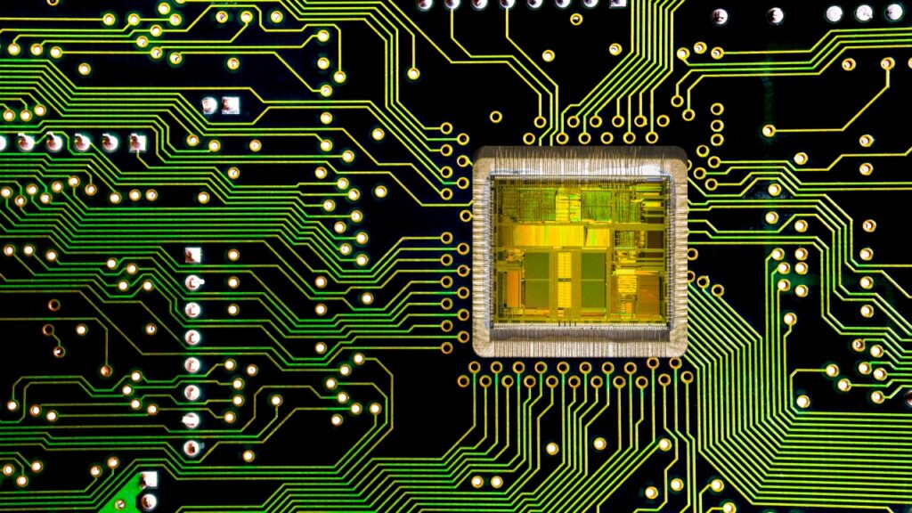
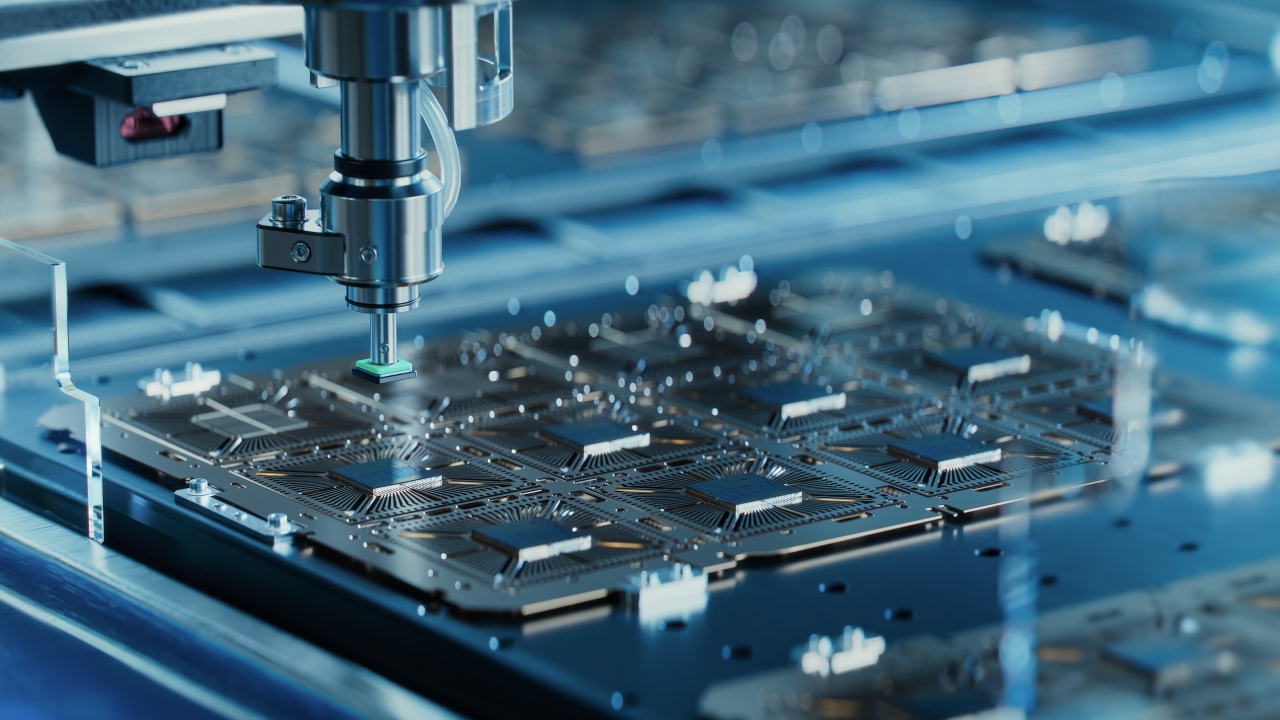
Packaging is a core technology that determines performance, reliability, and yield.
【2】The Changing Position of Packaging Technology
In the past:
● Chip performance = determined by process scaling
Today:
● Chip performance = process × packaging × memory × power × cooling
In AI and HPC in particular, situations in which packaging becomes the bottleneck are increasing rapidly.
【3】Key Keywords to Master from Chapter 6
The minimum keywords you should understand throughout Chapter 6 are as follows.
・Wire bonding / flip chip
・Fan-in / fan-out
・Thermal design (TIMs, heat spreaders, liquid cooling)
・SI / PI / EMI
・Reliability (thermal cycling, solder fatigue)
・HBM / chiplets / 2.5D
・ABF substrates, RDL
・KGD, package yield
・3D stacking, optical I/O
These are not separate pieces of knowledge; they are all interconnected.
【4】Important Perspectives as an Engineer
The most important thing in Chapter 6 is the sense that optimizing one factor alone does not work.
・Improving heat dissipation → increases stress
・Scaling down → reduces yield
・Increasing performance → makes power and EMI more difficult
Design decisions must always be made with an understanding of trade-offs.
【5】How Chapter 6 Connects to Chapter 7 and Beyond
The content covered in Chapter 6 centered on:
・Structures
・Materials
・Processes
However, in actual practice, the next challenges are:
・How to inspect them
・How to judge good or bad
・How to improve yield
→ This leads into Chapter 7: Inspection and Characterization Technology.
【6】Where This Knowledge Is Useful in Practice
The knowledge from Chapter 6 is directly useful in the following situations:
・Studying package structure specifications
・Isolating the causes of defects and complaints
・Technical discussions with material and equipment manufacturers
・Forming hypotheses when yield deteriorates
・Explaining why a particular structure is used
There are many areas where you cannot take part in the discussion without this knowledge.
【7】Summary
・Packaging is a core technology that determines performance
・In the era of AI and HBM, packaging is the main battleground
・It is an integrated technology of electrical, thermal, mechanical, and materials engineering
・It is directly linked to yield and cost
・In the future, it will evolve toward 3D, optics, and liquid cooling
Comprehension Check
1.Why has the importance of packaging technology increased so sharply in the era of AI chips?
2.Why does optimizing a single factor not work in package design?
3.Explain how the content of Chapter 6 connects to Chapter 7 (Inspection and Characterization Technology).
Column Supervisor: Koji Kakumoto (President, OTIS Co., Ltd.)
After studying abroad and working in planning and development at a trading company, he joined OTIS Co., Ltd. in 2011. While primarily working in the Corporate Planning Department, he has also served concurrently in manufacturing and technical divisions, and since 2018 has served as President, working to drive business growth and strengthen the organization.
This article is a general technical explanation intended for educational purposes and does not refer to any specific company, product, or technology.