【1】Why Interconnect Technology Became the Bottleneck of Scaling
Semiconductors have improved their performance through “transistor scaling,” but in recent years interconnects have become the main cause of performance degradation.
The reasons are as follows:
● The resistance of metal (Cu) wiring increases with scaling
● Parasitic capacitance between wires increases
● RC delay (resistance × capacitance) becomes dominant
● Greater complexity due to multilayer wiring (from 10 layers to 15 or more)
Particularly in AI / GPU / CPU chips, we are now in an era in which wiring delay, rather than the transistors, determines the performance of the entire chip.
【2】Why Low-k / Ultra Low-k Materials Were Introduced
To improve wiring delay (RC delay), the capacitance (C) must be reduced.
Capacitance is determined as follows:
C = ε × A / d (ε: dielectric constant)
In other words,
using a material with a low dielectric constant (Low-k) → capacitance decreases → delay decreases.
The materials have evolved from conventional SiO₂ (k≈4)
to Low-k (k≈2.7)
and Ultra Low-k (k≈2.2–2.4).
【3】Challenges of Low-k Materials and Countermeasures
To lower the dielectric constant, Low-k materials are often porous (structures containing air). As a result, the following challenges arise:
● Lower mechanical strength
● Film collapse during damascene CMP
● Degradation due to moisture absorption
● Cracking caused by heat and stress
● Delamination at the interface with metal
→ Reliability tends to drop significantly.
For this reason, the latest processes require numerous measures, such as:
・Combination with protective films such as SiCN
・Film strengthening through plasma treatment
・Pore sealing technology
・Conformal coating by ALD
【4】The Evolution of Multilayer Wiring (10 → 15 → 20 Layers)
As scaling progresses, the number of wiring layers continues to increase.
In leading-edge logic from Intel and TSMC:
● 10–12 layers: conventional
● 15 layers: becoming common
● 20 layers: under consideration for AI chips
Because higher wiring density and shorter wiring distances translate directly into higher performance, going multilayer has become unavoidable.
Challenges of Multilayer Wiring
・Accumulation of stress in the stacked structure
・Interlayer delamination due to differences in thermal expansion
・Insufficient strength of interlayer dielectric films
・Increased via resistance (the contact resistance problem)
Vias in particular are approaching the limit of how thin they can be as scaling continues, and we are now in an era in which contact resistance dominates transistor performance.
【5】The Evolution of the Damascene Process
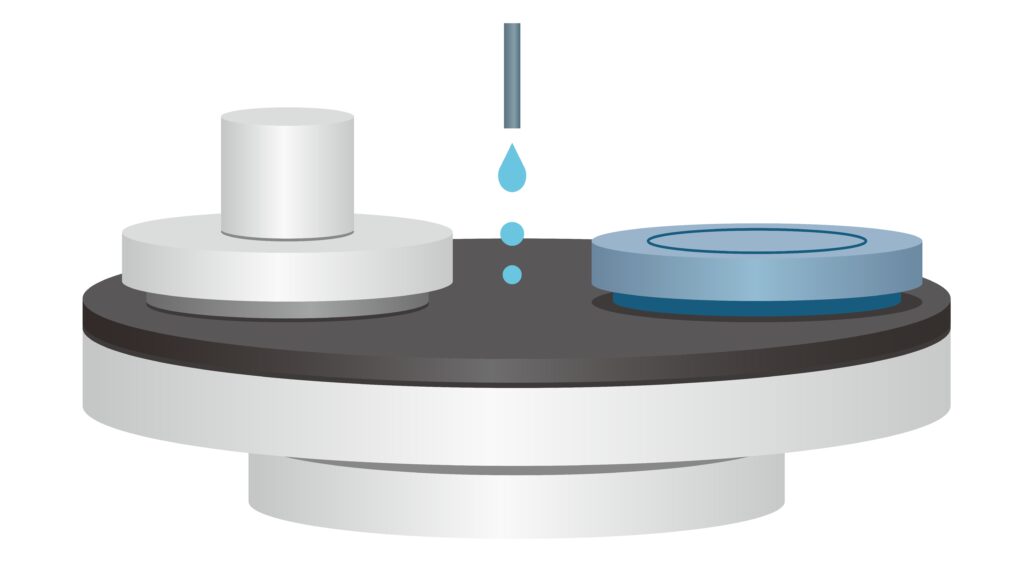
Dual damascene is used to form multilayer wiring.
Steps:
1.Etch trenches and vias into the Low-k film
2.Ta/TaN barrier film
3.Cu filling
4.Planarization by CMP
Challenges:
・Damage to and collapse of the Low-k film
・Cu diffusion
・Limits on thinning the barrier film
At advanced nodes, research into new materials is progressing, including:
・Barrierless materials such as Ru and Co
・Cu recrystallization technology
・ALD barrier films
【6】Future Directions (The Post-Low-k Era)
As the reliability of Low-k materials approaches its limits, the following new approaches are being considered:
● Air-gap structures (using air as the insulator)
● Shortening the wiring itself with hybrid bonding
● New materials other than Cu (intermetallic compounds, graphene)
● Backside power delivery
In particular, backside power delivery (BS-PDN) separates the power wiring onto the back side, greatly reducing the density of the front-side wiring, and is becoming a decisive solution to the wiring resistance problem.
【7】Summary
● Wiring delay (RC delay) is the biggest bottleneck in advanced processes
● Low-k reduces capacitance and improves wiring speed
● However, Low-k has low strength and many reliability challenges
● Multilayer wiring (10 → 15 → 20 layers) is essential for AI chips
● Damascene technology is pushing the limits of materials and processes
● New structures such as backside power delivery and hybrid bonding are emerging
Comprehension Check
1.Explain why using Low-k materials reduces wiring delay.
2.Name two typical weaknesses of Low-k materials.
3.What challenges arise as the number of wiring layers increases?
Column Supervisor: Koji Kakumoto (President, OTIS Co., Ltd.)
After studying abroad and working in planning and development at a trading company, he joined OTIS Co., Ltd. in 2011. While primarily working in the Corporate Planning Department, he has also served concurrently in manufacturing and technical divisions, and since 2018 has served as President, working to drive business growth and strengthen the organization.
This article is a general technical explanation intended for educational purposes and does not refer to any specific company, product, or technology.