【1】Why Chiplets Became Necessary
Conventional large-scale SoCs have a major problem: yield and manufacturing cost.
The larger a chip becomes:
・The probability of defects increases
・Yield decreases
・Manufacturing costs rise sharply
In other words, the larger the single chip you make, the higher the manufacturing risk.
With chiplets, chips are divided by function, so the size of each chip can be reduced and yield can be improved.
【2】The Basic Structure of Chiplets
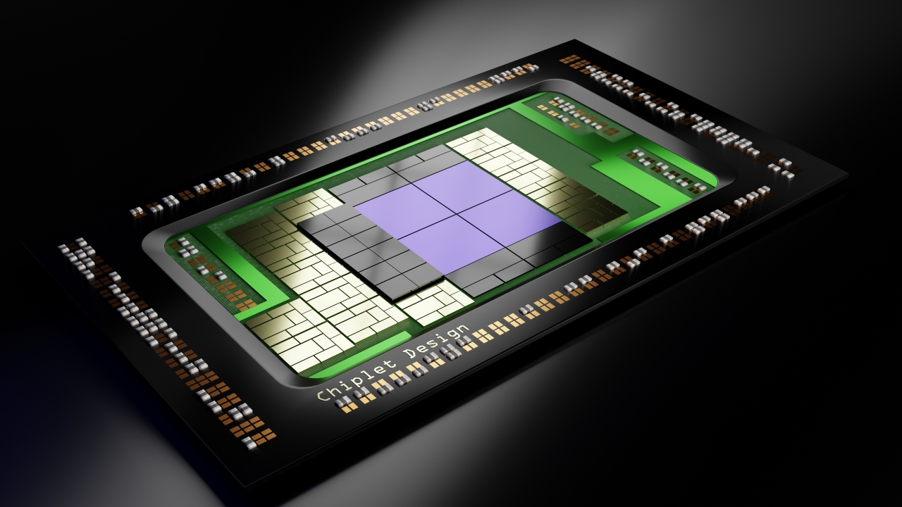
In chiplet design, multiple chips are placed within a single package and connected by high-speed interconnects.
Typical configuration:
・CPU chiplets
・GPU chiplets
・I/O chiplets
・Memory interfaces
These are connected inside the package and operate as a single processor.
【3】Advantages of Chiplets
Chiplet architecture has many advantages.
Main advantages:
・Improved yield
・Greater design reusability
・Lower development costs
・Combining different process nodes
For example, it becomes possible to manufacture the compute portion with a leading-edge process and the I/O portion with a mature process.
【4】Actual Adoption Examples
Chiplets have already been adopted by many semiconductor companies.
Representative examples:
・AMD EPYC (CPU chiplet structure)
・Intel EMIB / Foveros
・Apple M series (advanced package integration)
In data center CPUs in particular, chiplet structures are becoming mainstream.
【5】Challenges in the Chiplet Era
On the other hand, chiplets also bring new challenges.
Main challenges:
・Faster chip-to-chip connections
・Power efficiency
・More complex package design
・Thermal management
In other words, in the chiplet era, not only transistor design but also packaging technology holds the key to performance.
For this reason, advanced packaging technology is rapidly growing in importance in the semiconductor industry.
【6】Summary
・Chiplets are a design method that combines multiple chips
・They can solve the yield problem of huge SoCs
・Different process nodes can be combined
・The importance of packaging technology increases even further
Comprehension Check
1.What kind of design method is chiplet architecture?
2.Why does yield become a problem with huge SoCs?
3.Why does packaging technology become important in the chiplet era?
Column Supervisor: Koji Kakumoto (President, OTIS Co., Ltd.)
After studying abroad and working in planning and development at a trading company, he joined OTIS Co., Ltd. in 2011. While primarily working in the Corporate Planning Department, he has also served concurrently in manufacturing and technical divisions, and since 2018 has served as President, working to drive business growth and strengthen the organization.
This article is a general technical explanation intended for educational purposes and does not refer to any specific company, product, or technology.