【1】What Is Wafer-Level Electrical Characteristic Testing?
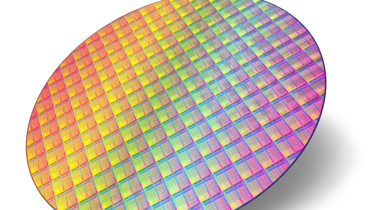
Wafer-level electrical characteristic testing refers to testing that measures electrical characteristics while still in wafer form, before the chips are cut out.
The purpose is clear: to judge at an early stage
・Whether transistors are operating as designed
・Whether process variation is within the allowable range
・Whether it is acceptable to proceed to volume production
If abnormalities are not caught here, the back-end becomes a gamble.
【2】Why Test at the Wafer Stage?
The reason is simple: the earlier a defect is found, the more cheaply it can be stopped.
The further the product moves into the back-end, the more the following accumulate:
・Processing costs
・Assembly costs
・Test costs
If it is stopped at the wafer stage:
・Losses are minimal
・Causes are easier to trace
・Process corrections are faster
E-Test is a breakwater that minimizes the factory’s losses.
【3】Main Electrical Characteristics Measured
What wafer testing looks at is not “works / doesn’t work” but trends.
Typical examples:
・Threshold voltage (Vth)
・Leakage current (Ioff)
・Drive current (Ion)
・Resistance and capacitance (R/C)
・Transistor variation
What matters is distribution and change rather than absolute values.
Even if the average is correct, volume production is risky if the distribution is wide.
【4】The Role of PCM (Process Control Monitor)
At the core of E-Test is the PCM (process control monitor device).
A PCM is an evaluation structure that is
・Separate from the product circuit
・Intended to visualize the process state
・Deliberately placed
Its roles are to:
・Detect deviations in each process
・Monitor day-to-day, lot-to-lot, and tool-to-tool differences
・Provide the basis for SPC data
A factory with a broken PCM is like driving blindfolded.
【5】Measurement Equipment and the Difficulty of Measurement
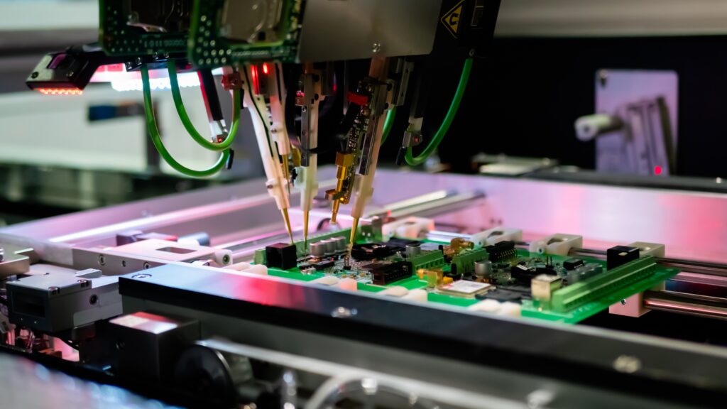
Wafer testing uses:
・Wafer probers
・High-precision probe cards
・Parameter analyzers
However, the difficulty is not the equipment.
・Probe contact resistance
・Contact position misalignment
・Surface damage
・Measurement noise
The measurement itself can create new variation.
Accidents in which you think you are measuring but are actually causing damage are not uncommon.
【6】How E-Test Data Is Used
The value of E-Test is determined by how it is used after measurement.
Examples of use:
・Correcting lithography conditions
・Fine-tuning ion implantation doses
・Optimizing deposition thickness
・Early detection of equipment abnormalities
E-Test is the starting-point data for process improvement.
【7】Why E-Test Becomes Difficult in Leading-Edge Processes
The more scaling advances, the more difficult E-Test becomes.
Reasons:
・Differences on the nm scale directly affect characteristics
・Increasing random variation
・Measurement points are limited in 3D structures
・Stochastic defects originating from EUV
There are more and more situations in which measurements cannot uniquely determine the cause.
For this reason, E-Test × statistics × AI analysis has become essential.
【8】Summary
・Wafer-level electrical characteristic testing is the first gate
・The earlier defects are stopped, the cheaper it is
・Look at distributions and trends rather than absolute values
・PCM is the cornerstone of process control
・At advanced nodes, analytical capability is competitiveness
Comprehension Check
1.Why is E-Test considered more important than back-end testing?
2.What is the role of the PCM?
3.Why can it be risky even if the average value is correct?
Column Supervisor: Koji Kakumoto (President, OTIS Co., Ltd.)
After studying abroad and working in planning and development at a trading company, he joined OTIS Co., Ltd. in 2011. While primarily working in the Corporate Planning Department, he has also served concurrently in manufacturing and technical divisions, and since 2018 has served as President, working to drive business growth and strengthen the organization.
This article is a general technical explanation intended for educational purposes and does not refer to any specific company, product, or technology.