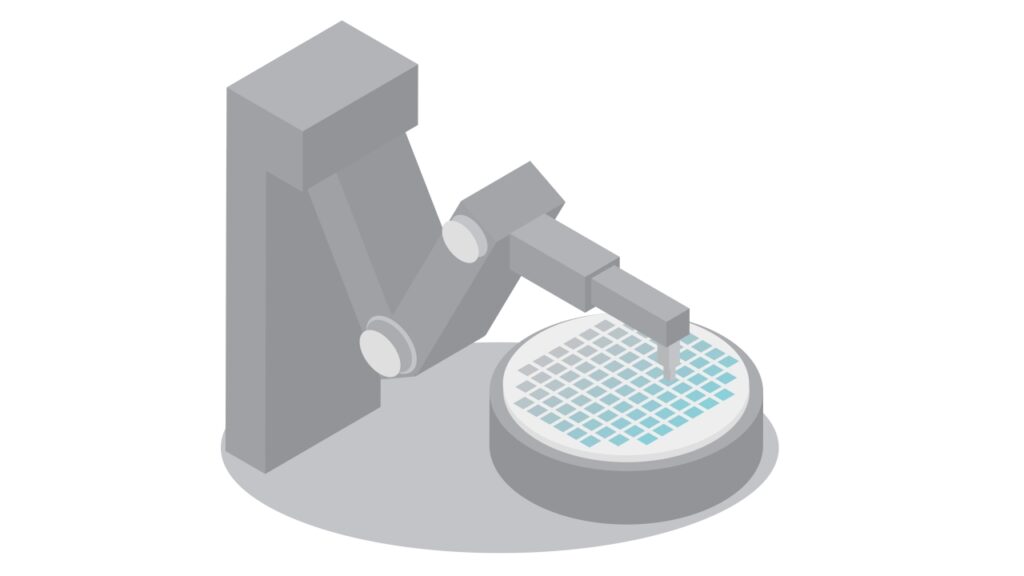
【1】What Is Visual Inspection?
Visual inspection refers to inspection that observes the physical condition of chips and packages and determines whether defects are present.
Its scope is broad.
・Wafer surfaces
・Wiring patterns
・Bumps
・Wire bond joints
・Mold resin
・Substrate joints
In other words, it is an inspection that exists across the entire process, from front-end to back-end.
【2】Why Visual Inspection Is Important
The reason is simple.
Physical defects turn into electrical failures with a time lag.
Examples:
・Microcracks → expand with temperature cycling
・Foreign particle adhesion → increased leakage current
・Missing wiring → EM failure
・Mold delamination → moisture-related degradation
Visual defects are also defects that work now but will fail in the future.
【3】Main Defects Targeted
Typical visual defects are as follows.
Particles (Foreign Matter)
・Dust
・Metal powder
・Resist residue
In fine wiring, a single particle can cause a short-circuit failure.
Scratches
・CMP scratches
・Handling scratches
・Probe scratches
A cause of wiring disconnection and reduced reliability.
Cracks
・Dicing cracks
・Cracks around bumps
・Mold cracks
They tend to propagate with temperature changes.
Delamination
・Interfaces between resin and chip
・Interfaces between RDL and insulating film
A cause of increased thermal resistance and moisture-related degradation.
【4】Inspection Equipment and Methods
Visual inspection mainly uses optical technology.
Typical equipment:
・Optical microscopes
・Automated optical inspection systems (AOI)
・High-resolution line scanning
・3D profile measurement systems
There are two main inspection methods.
Manual Visual Inspection
・A person observes with a microscope
・Strong at detecting subtle defects
However,
・It requires many man-hours
・Results vary between individuals
There are limits in volume production.
Automated Optical Inspection (AOI)
・Image acquisition
・Image comparison
・Defect extraction
Enables high-speed, high-volume inspection. The current mainstream.
【5】AOI Judgment Logic
AOI is not simple image comparison.
Typical methods:
・Golden sample comparison
・Pattern recognition
・Brightness difference analysis
・Edge detection
The more scaling advances, the more blurred the difference between normal and abnormal becomes.
Optimizing false alarms and escapes (missed defects) is a challenge.
【6】The Difficulty of Visual Inspection in Advanced Packaging
In advanced packaging, the difficulty rises sharply.
Reasons:
・Finer bumps
・Multilayer RDL
・3D stacked structures
・Internal defects that light cannot reach
For this reason, it is combined with non-destructive internal inspection such as:
・X-ray inspection
・CT inspection
・Ultrasonic inspection
【7】Use of Visual Inspection Data
Visual inspection does not end with judgment.
Examples of use:
・Defect mapping
・Detecting equipment abnormalities
・Identifying transport system problems
・Understanding process variation
Defect maps are one of the most important data sources for yield improvement.
【8】Summary
・Visual inspection is a basic inspection that captures physical defects
・Many defects appear as physical shapes
・AOI is the mainstream in volume production
・Internal inspection is essential in advanced packaging
・Defect maps are key to process improvement
Comprehension Check
1.Why do visual defects turn into electrical failures with a time lag?
2.What is the difference between AOI and manual visual inspection?
3.List the reasons why optical inspection is difficult in advanced packaging.
4.What are defect maps used for?
Column Supervisor: Koji Kakumoto (President, OTIS Co., Ltd.)
After studying abroad and working in planning and development at a trading company, he joined OTIS Co., Ltd. in 2011. While primarily working in the Corporate Planning Department, he has also served concurrently in manufacturing and technical divisions, and since 2018 has served as President, working to drive business growth and strengthen the organization.
This article is a general technical explanation intended for educational purposes and does not refer to any specific company, product, or technology.